01Mate80Chip Landscape: A Precise Balance of Yield and Performance
The unprecedented “three-chip” strategy of the Huawei Mate80 series reflects a profound understanding of semiconductor manufacturing principles.
The base model is equipped with the Kirin 9020 chip, achieving a balance of “high yield and low cost” through mature processes, allowing for a starting price of 4699 yuan;
As the absolute main character, the Kirin 9030, with a frequency of 2.75GHz and Mailoon935 GPU, has achieved breakthroughs in leakage control and voltage management with domestic technology;
The Kirin 9030Pro, exclusive to the ProMax model, achieves performance upgrades through “wafer core area selection,” ensuring stability under high-load scenarios.
The precise division of these three chips essentially utilizes “manufacturing differences” in a refined manner — and the first checkpoint for discovering these differences is the semiconductor probe.
 02Test Probes: The “Millimeter Experience” for Chips
In the journey of Kirin chips from wafer to finished product, test probes play an irreplaceable role as “quality gatekeepers.” To understand their importance, one must first grasp their precise structure.
1. The Precise Structure of Probes
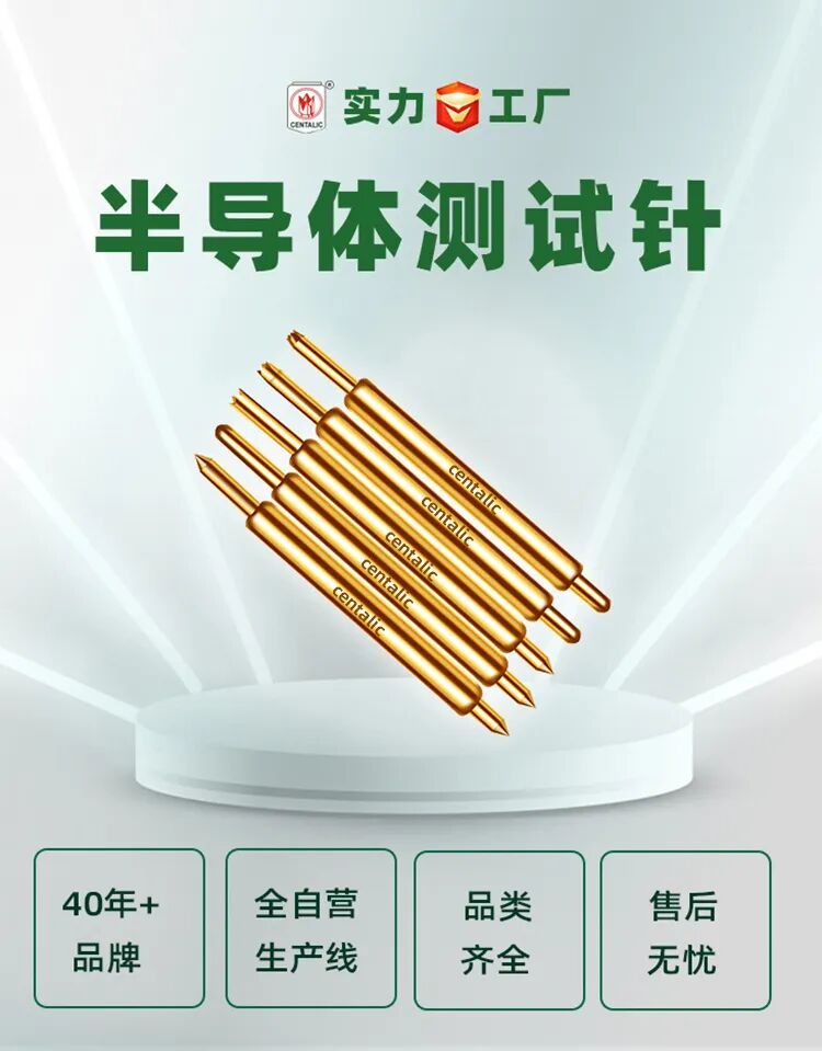
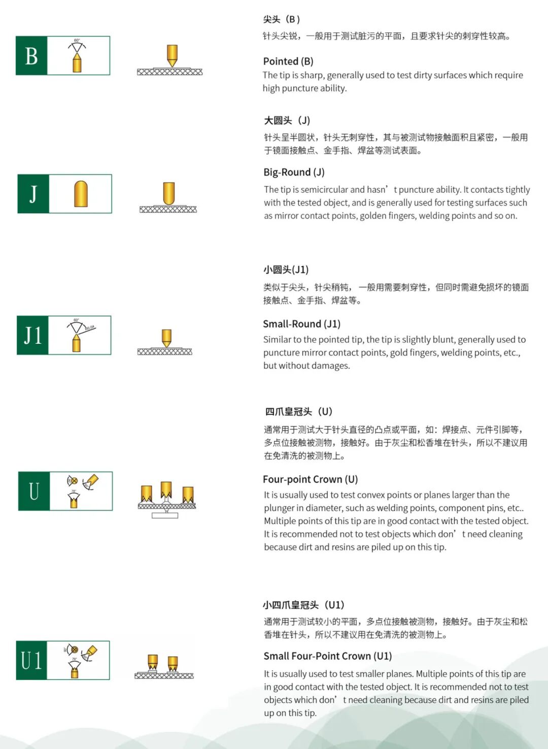
A semiconductor probe is a high-end precision electronic component, also known as a “dual-head test probe.” Structurally, it generally consists of three basic components: the probe tip, probe tube, and spring, which are formed through precision instruments and pre-pressing. They can be categorized into series such as dual-head single-action probes and dual-head double-action probes. Common inner probe tip types include B, J, J1, U, U1, etc. Due to the extremely small size of semiconductor products, especially chips, the probe size must reach the micrometer level.
2. The Role of Probes: Precise Touch and Signal Transmission
The core function of test probes is to establish a physical connection with the chip through the tiny probe tip after the chip manufacturing is complete, transmitting test signals to the chip and reading feedback data. This process not only verifies whether the chip functions normally but also detects potential manufacturing defects. It can be said that every successfully shipped chip relies on tens of thousands of “precise touches” from test probes.
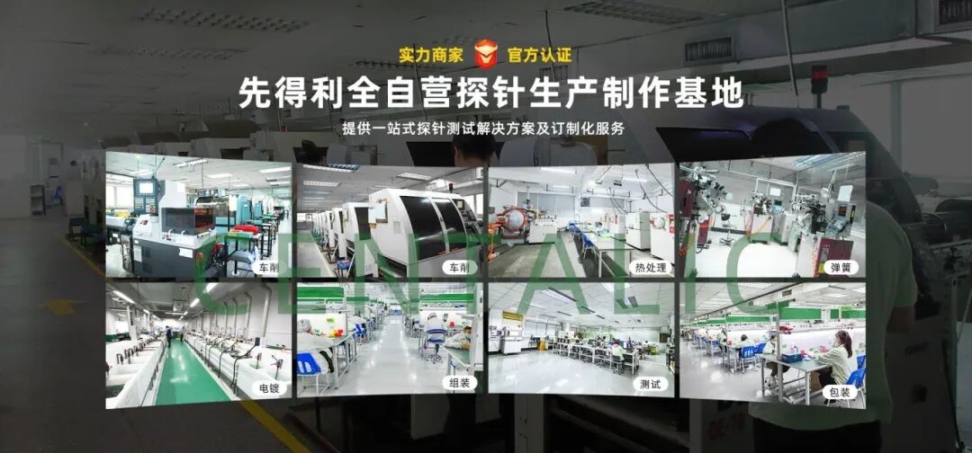
Supporting this “precise touch” requires an accumulation of knowledge regarding probe structure and processes. Shendi, as a national high-tech enterprise with over 40 years of experience and a “fully self-operated large-scale” probe production line, focuses on the research and manufacturing of various test probes. By carefully selecting high-quality materials, optimizing coating processes, and employing precision assembly techniques, these test probes can achieve a minimum diameter of: probe tip φ: 0.06mm/probe tube φ: 0.10mm.

3. Three Key Applications of Probes in Mate80 Chips
For the Mate80 series, the detection by test probes directly determines the performance grading and cost control of the final product:
Yield Screening:The high yield of the Kirin 9020 benefits from early screening by test probes, which can quickly eliminate chips with excessive leakage or circuit anomalies, avoiding subsequent ineffective packaging costs.
Performance Grading:The distinction between 9030 and 9030Pro relies on test probes accurately capturing the power consumption and signal stability of the chip under high load across a wide temperature range. Outstanding “potential stocks” are marked as 9030Pro for high-end models.
Process Validation:The high-frequency breakthroughs of the Kirin 9030 are backed by “stress tests” conducted by test probes on new domestic processes, validating the reliability of transistor leakage control technology through simulated extreme scenarios.
03The Future on the Tip of the Needle: A Necessary Answer for High-End Development
As chip processes advance below 3nm and 3D packaging technology becomes widespread, test probe technology faces the challenges of “three supers”:super dense spacing, super high frequency, and super long lifespan. This is not only a topic for probe manufacturers but also requires deep collaboration with chip design stages. For Huawei, which aims to reach the top, mastering and leading this set of precise testing language will be a necessary answer for whether its future flagship can maintain a leading edge.
For more exciting content, follow our WeChat public account below!