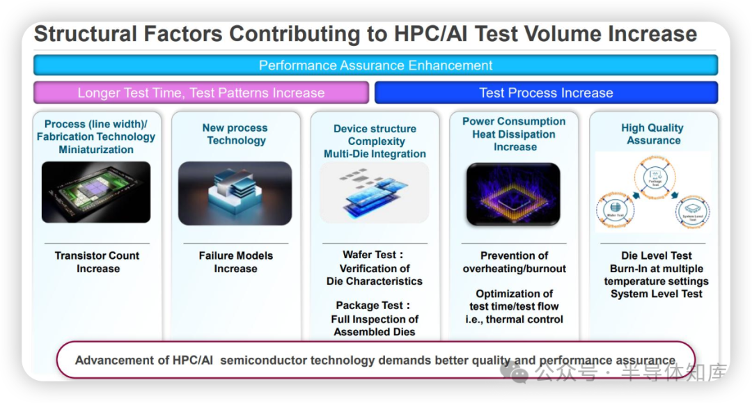
1. The Evolution of AI Chip Technology and Its New Demands on Semiconductor Equipment
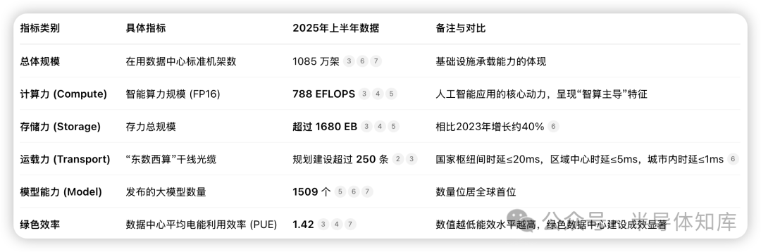 As of the end of June 2025, the core quantitative indicators of computing power development in China
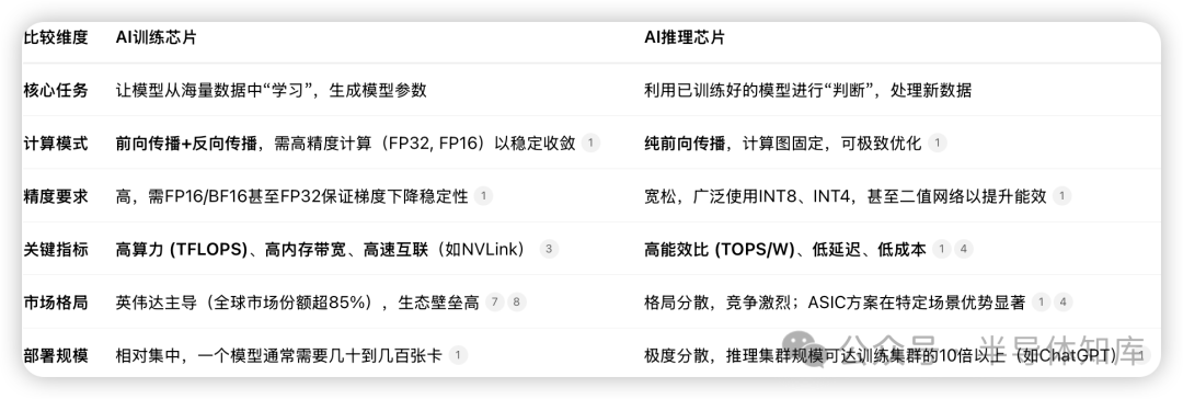
The rapid development of AI chip technology is imposing unprecedented technical requirements on semiconductor back-end equipment. Compared to traditional chips, AI chips exhibit significant differences in process technology, packaging technology, and testing requirements, which directly drive back-end equipment to upgrade towards higher precision, higher integration, and higher speed.
🚀 Testing Challenges Brought by Process Technology Upgrades
The widespread adoption of advanced processes has led AI/HPC chips to gradually adopt advanced processes such as 4nm. Taking NVIDIA’s Blackwell GPU as an example, its transistor density reaches 208 billion, resulting in a significant increase in chip complexity and power consumption. This change imposes higher requirements on back-end testing equipment:
- Surge in testing volume and time: The high integration and stability requirements of AI chips lead to a substantial increase in the number of test vectors and scan tests, with scan test coverage needing to reach 95%-99.5%
- Increased structural complexity: Transitioning from FinFET to GAA (Gate-All-Around) structures, the future 2nm process may adopt CFET technology, introducing new failure nodes and testing challenges
💡 New Requirements for Equipment from Advanced Packaging Technology
HBM (High Bandwidth Memory) + CoWoS (2.5D packaging) has become a key solution for AI chips, supporting high-speed interconnection between GPUs and HBM. This advanced packaging technology has a profound impact on back-end equipment:
- Demand for 2.5D/3D packaging: Requires TSV (Through-Silicon Via), RDL (Redistribution Layer), bump technologies to achieve multi-layer chip stacking (such as 8-layer DRAM stacking for HBM)
- Increased integration: Chiplet design requires individual testing (Die Level Test) for each small chip and system-level collaborative verification
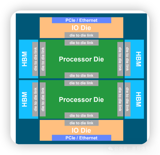 HPC/AI chips typically integrate multiple processors, I/O chips, and HBM memory
⚡ Comprehensive Upgrade of Testing Equipment Technical Indicators
Significantly increased requirements for testing accuracy and speed, back-end testing equipment needs to meet the unique high-performance demands of AI chips:
| Technical Indicators | Traditional Chip Requirements | New Requirements for AI Chips |
|---|---|---|
| Testing Speed | General functional testing | Support high-speed signals (e.g., HBM testing speed up to 9Gbps) |
| Parallel Processing Capability | Basic channel count | High parallel processing (channel count exceeding 16,000) |
| Timing Accuracy | Regular accuracy | Low latency (timing accuracy ±45 picoseconds) |
| Power Requirements | Standard power supply | Testing machines need to provide over 2000A current |
🔧 Significant Increase in Packaging Equipment Precision Requirements
Bonding technology is shifting from wire bonding to hybrid bonding, resulting in a qualitative change in precision requirements:
- Precision improvement: From traditional 20μm precision to 0.1μm level
- I/O density increase: From 5/mm² to 10k+/mm²
- Thinning requirements: Wafer thickness needs to be reduced from 150μm to below 30μm, TTV (Total Thickness Variation) < 1μm
📊 Comparison of AI Chips and Traditional Chip Technology Differences
| Dimension | Traditional Chips | AI Chips |
|---|---|---|
| Process Technology | Mostly using processes above 14nm, with lower transistor density | Generally using processes of 7nm and below, with extremely high transistor density |
| Packaging Technology | Mainly using wire bonding, with simple structures | Relying on 2.5D/3D advanced packaging, requiring TSV, RDL, and other technologies |
| Testing Complexity | Low testing volume, mainly basic functional testing | Testing volume surges (scan testing volume increases by 1500 times), requiring multi-stage testing |
| Storage Requirements | Standard DRAM/GDDR memory, with lower bandwidth | HBM memory has become mainstream, with bandwidth reaching 4.8TB/s |
🎯 Summary: Upgrade Directions for Back-End Equipment Technology
The evolution of AI chip technology drives back-end equipment to upgrade in three major directions:
- Testing Equipment focuses on enhancing parallel channel count, timing accuracy, and power supply capability
- Packaging Equipment focuses on hybrid bonding precision, ultra-thin wafer processing, and integration of advanced packaging processes
- Technical Barriers are concentrated on self-developed ASIC chips and specialized process modules, with overseas leaders still dominating the high-end market
These new demands present significant opportunities for domestic back-end equipment manufacturers while also posing higher technical challenges. The technical barriers for equipment are mainly concentrated in self-developed ASIC chips (such as the main control chip for testing machines) and specialized process modules (such as copper plating filling and deep hole etching), with overseas leading companies like Advantest and DISCO still dominating the high-end market, and the localization process urgently needs breakthroughs.
2. Upgrading Technical Indicators of Back-End Equipment Under the Rise of Domestic Computing Power
As domestic AI chips like Huawei’s Ascend 910B achieve performance parity with NVIDIA’s A100, the domestic computing power industry chain imposes stricter technical requirements on back-end equipment. Compared to traditional international manufacturers, domestic AI chip manufacturers have higher requirements for pin counts, current carrying capacity, etc., driving back-end equipment to comprehensively upgrade towardshigh performance, high precision, and high integration in three major directions.
🔌 Testing Equipment: Evolving from Basic Functionality to High-Speed and High-Parallelism
SoC testing machines have undergone a qualitative leap in technical indicators:
- Pin scale: Must support thousands of pins, far exceeding traditional chip testing requirements
- Testing speed: Digital channel speed requirements have increased from 100MHz to 1.6GHz
- Vector depth: Must reach 256-512MV deep vector storage capacity to cope with complex fault models of AI chips
- Current carrying capacity: Power supply capability must be increased to 1000-2000A to meet the low voltage and high power characteristics of advanced process chips
Storage testing machines have special requirements for HBM testing:
- Channel scale: Parallel channel count must exceed 16,000 (e.g., Advantest T5503HS2 model)
- Data rate: Must support high-speed signal testing up to 36Gbps
- Timing accuracy: Requires precise timing control of ±45 picoseconds to ensure the reliability of multi-die collaborative testing
Technical Difference Comparison:
| Indicator Dimension | International Manufacturer Standards | Domestic AI Chip Requirements |
|---|---|---|
| Testing Speed | Advantest V9300 supports >800Mbps | Requires customized boards to support higher speeds |
| Chip Solutions | Self-developed ASIC chips for high-speed testing | Short-term reliance on FPGA solutions (limited to 800Mbps) |
| Testing Process | Covers all testing stages | Emphasizes cost control and rapid iteration |
🏭 Packaging Equipment: Precision Requirements Show an Order of Magnitude Increase
Thinning equipment faces challenges in ultra-thin processing:
- Thickness indicators: Wafer thickness must be reduced from 150μm to below 30μm, TTV (Total Thickness Variation) requirements < 1μm
- Surface quality: Surface roughness Rz must be < 0.01μm to avoid micro-crack generation
- Processing yield: Addressing the issue of ultra-thin wafers being prone to damage, improving batch production stability
Bonding equipment is upgrading to hybrid bonding:
- Precision leap: From traditional 20μm precision to 0.1μm hybrid bonding precision
- Density breakthrough: I/O connection density has increased from 5/mm² to 10k-100k interfaces/mm²
- Energy efficiency optimization: Energy consumption requirements < 0.05pJ/bit to meet high-density interconnect energy efficiency needs
Electroplating equipment faces technical barriers:
- Deposition quality: TSV copper filling must achieve defect-free deposition to ensure electrical reliability
- Process uniformity: Bump production must achieve nano-level thickness uniformity control
- Current scale: Electroplating current must reach 1000-2000A levels
🚧 Technical Barriers and Domestic Breakthrough Paths
Core bottlenecks in the testing phase:
- Reliance on ASIC chips: PE/TG chips are monopolized by ADI/TI, with long self-development cycles (e.g., Huafeng Measurement Control STS8600 development)
- Algorithm software shortcomings: Insufficient accumulation of testing vector generation software like SmartTest
- High parallel testing: HBM testing requires over 1024 DUTs to be tested simultaneously, while domestic equipment channel counts have not yet fully matched
Technical leaps in the packaging phase:
- Integration of front-end processes: Advanced packaging requires the introduction of PVD/CVD, photolithography, and other front-end equipment, with a significant technical gap
- Material precision challenges: Ultra-thin wafer thinning is prone to cracking, and hybrid bonding requires nano-level alignment precision
- Equipment collaboration challenges: HBM manufacturing requires integration of thinning-bonding-electroplating multi-equipment production lines, lacking overall solution experience
Progress of domestic equipment:
- Huafeng Measurement Control STS8600: Breakthrough of 800Mbps bottleneck through self-developed ASIC chips, currently in customer verification stage
- Huahai Qingke Versatile-GP300: The first domestic 12-inch thinning machine integrating grinding and CMP, TTV < 1μm, has been delivered to leading customers
- Tuojing Technology hybrid bonding equipment: Dione 300 series achieves room temperature multi-material surface bonding, has received repeat orders
The rise of domestic computing power is forcing a comprehensive upgrade of back-end equipment technical indicators, but there are still significant gaps in core chips, front-end process integration, and high-end equipment localization. Equipment manufacturers need to achieve breakthroughs in self-developed ASIC chips, hybrid bonding, and other key areas to meet the increasingly complex technical demands of AI chips.
3. In-Depth Analysis of Key Breakthrough Points in Back-End Equipment Technology
As AI chips rapidly evolve towards advanced processes of 4nm and below, and 2.5D/3D packaging architectures, back-end equipment faces unprecedented technical challenges. Currently, domestic equipment is accelerating breakthroughs in core areas such as self-developed ASIC chips for testing machines, hybrid bonding precision control, and ultra-thin wafer processing, gradually narrowing the gap with international leaders.
🔬 Testing Equipment: Dual Breakthroughs in High-End SoC and Storage Testing
1. SoC Testing Machines – Self-Developed ASIC Chips as the Key to Breakthrough
- Huafeng Measurement Control STS8600: As a core product entering the high-end SoC testing market, it has achieved technical benchmarking against Advantest V9300K model. This equipment features4000+ digital channels,2000A power supply capability, and1.5G vector storage space, specifically designed for high-power chips like AI/GPU.
- Focus of Technical Breakthroughs:
- Replacing FPGA with self-developed ASIC chips: Current FPGA architecture is limited to 800Mbps, while 1.6GHz testing requires dedicated ASICs. Huafeng Measurement Control has initiated a self-developed ATE chip project aimed at breaking through high-speed testing bottlenecks.
- Multi-Protocol Compatibility and High Parallel Architecture: Supports complex protocols such as scan testing and functional testing, requiring the construction of a hardware platform for testing over 1024 DUTs to match the pin scale of AI chips.
- Industrial Progress: STS8600 has received its first order from Tsinghua University in December 2024 (unit price 4.47 million yuan) and is currently undergoing verification with leading customers such as Haiguang Information and Biran Technology, with an expected new order of 350-400 million yuan by 2026.
2. Storage Testing Machines – Increased Complexity of HBM Testing
- Technical Parameter Leap: HBM testing must meet36Gbps data rates,16000+ channels of parallel processing, and ±45ps timing accuracy, with current carrying requirements reaching 1000-2000A.
- Domestic Gaps: Models like Advantest T5503HS2 dominate the high-end market, while domestic equipment still has shortcomings in areas like TG/PE chips (relying on ADI/TI) and SmartTest algorithm software.
- Partial Breakthroughs: Wuhan Jinghong’s aging testing products have entered the Yangtze Memory supply chain, and Changchuan Technology’s D9000 testing machine is designed specifically for Chiplet architecture, supporting multi-chip collaborative testing, with orders from Samsung Electronics and Huawei expected in 2025.
🧩 Packaging Equipment: Hybrid Bonding and Ultra-Thin Processing Lead Upgrades
1. Thinning Machines – Tackling Ultra-Thin Wafer Batch Processing Challenges
- Technical Barriers: AI chip packaging requires wafer thickness < 30μm, total thickness variation (TTV) < 1μm, and surface roughness Rz < 0.01μm to avoid micro-cracks that lead to yield loss.
- Huahai Qingke Versatile-GP300: The first domestic 12-inch thinning machine integrating grinding and CMP, TTV < 1μm, has been delivered to leading customers. ItsVersatile-GM300 thinning and film integration machine is also compatible with W2W/D2W processes, with mass shipments expected in the first half of 2025.
- Benchmarking Gaps: Japan’s DISCO thinning machines hold over 50% of the global market share, while domestic equipment still needs to catch up in automation precision and production capacity (e.g., monthly production of 10,000 pieces).
2. Bonding Machines – Hybrid Bonding Precision Approaching Nano-Level
- Technical Iteration: Traditional wire bonding precision is 20μm, while hybrid bonding needs to improve to0.1μm, with I/O density increasing from 5/mm² to10k+/mm².
- Tuojing Technology Breakthrough:
- Dione 300 series: Achieves W2W hybrid bonding, has received repeat orders from customers, and the room temperature multi-material bonding technology is entering the industrialization stage.
- Pleione 300: Designed for HBM and three-dimensional chip integration, expected to ship and verify smoothly in the first half of 2025, with alignment precision approaching that of leading international levels like EVG.
- Market Landscape: Global bonding equipment is dominated by EVG (59% share) and SUSS, while Tuojing Technology leads domestic installations due to HBM mass production orders.
3. Electroplating and Patterning Equipment – TSV Filling and Front-End Process Integration
- Electroplating Process Bottlenecks: TSV copper filling must achieve defect-free deposition, with current carrying reaching 1000-2000A. Shengmei Shanghai holds about 1.5% of the back-end electroplating equipment market, but front-end equipment is monopolized by LAM/AMAT (96% share).
- Front-End and Back-End Collaboration Challenges: RDL wiring and TSV drilling require the introduction of PVD/CVD, photolithography, and other front-end equipment, with domestic companies lacking integrated process experience.
📊 Comprehensive Evaluation of Technical Breakthroughs
| Equipment Type | International Leader Technical Indicators | Domestic Breakthrough Status | Key Gaps |
|---|---|---|---|
| SoC Testing Machines | Advantest V9300: 1.6Gbps channels, self-developed ASIC | Huafeng Measurement Control STS8600: 800Mbps, ASIC development ongoing | High-speed chips rely on imported PE/TG chips |
| Storage Testing Machines | Advantest T5503HS2: 16,000 channels, 36Gbps | Changchuan Technology D9000: Supports multi-chip testing for Chiplet | High channel count hardware architecture is not mature |
| Thinning Machines | DISCO: TTV < 0.5μm, monthly production capacity of 10,000 pieces | Huahai Qingke GP300: TTV < 1μm, batch delivery | Automation precision and production stability |
| Hybrid Bonding Machines | EVG: Alignment precision 0.1μm, bonding strength >200MPa | Tuojing Technology Dione 300: Received HBM mass production orders | Process coverage and long-term reliability |
💡 Outlook on Breakthrough Paths
Domestic back-end equipment needs to accelerate breakthroughs along three major paths:
- Core Chip Autonomy: Prioritize overcoming “bottleneck” areas such as testing machine ASICs and bonding machine nano-level positioning chips.
- Process Module Integration: Promote the integration of thinning-bonding-electroplating multi-equipment production lines to solve front-end and back-end collaboration challenges.
- Algorithm Software Ecosystem: Develop testing vector generation tools like SmartTest to fill the software-defined equipment gap.
Currently, companies like Huafeng Measurement Control, Changchuan Technology, and Tuojing Technology have moved from customer verification to small batch orders, but the replacement rate in the high-end market is still below 10%. As AI chip iterations accelerate, breakthroughs in back-end equipment technology will become a decisive battle for the autonomy and controllability of the domestic computing power industry chain.
4. Technical Roadmap and Industrialization Timeline Predictions
(Note: Based on the document content, the report does not provide a clear technical roadmap and timeline predictions; the following information is an objective description of existing progress)
1. AI Chip Technology Evolution Nodes
The document shows that AI/HPC chips have widely adopted 4nm processes (such as NVIDIA’s Blackwell GPU) and mentions that the next generation of technology direction is GAA (Gate-All-Around) structures, with the 2nm node possibly adopting CFET technology. However,no specific mass production timetable or evolution milestones are provided.
2. Progress in Back-End Equipment Technology Breakthroughs
-
Testing Equipment
- Huafeng Measurement Control STS8600: Received its first order from Tsinghua University in December 2024 (unit price 4.47 million yuan), currently in multi-customer verification stage, with an expected new order of 350-400 million yuan by 2026.
- Changchuan Technology D9000: Has received orders from Samsung, Huawei, and domestic AI chip manufacturers, supporting multi-chip collaborative testing, but has not disclosed batch delivery timelines.
Packaging Equipment
- Thinning Machines: Huahai Qingke Versatile-GP300 has been delivered to leading customers, and Versatile-GM300 is expected to be mass-produced in the first half of 2025; the three-axis thinning and polishing machine from Jing Sheng Machine Electric is in demo stage.
- Bonding Machines: Tuojing Technology Dione 300 series has received repeat orders from HBM customers, and Pleione 300 is expected to ship and verify smoothly in the first half of 2025, but no large-scale installation timeline has been provided.
3. Judging the Industrialization Stage
- Current Status: The localization rate of high-end back-end equipment is still below 10%, and the overall situation is in the transition stage ofcustomer verification → small batch orders.
- Key Window Period: 2025-2026 is seen as an important period for the large-scale verification and order fulfillment of domestic equipment, but the document does not provide specific time predictions for the overall maturity of the industrial chain.
4. Lack of Process Node Planning
The document only mentions the development of AI chips towards advanced processes (such as 4nm) and does not cover detailed evolution routes, trial production, or mass production plans for future nodes like 2nm and 1nm.
Conclusion: The report has significant information gaps in the dimensions of technical roadmap and timeline, and the industrialization process needs to rely on real-time tracking of enterprise dynamics.
5. Latest Verification and Mass Production Progress of Companies like Huafeng Measurement Control and Changchuan Technology
Huafeng Measurement Control STS8600 testing machine has entered a critical customer verification period, successfully winning the Tsinghua University high-speed memory automatic testing system project in December 2024 (unit price 4.47 million yuan), marking the first order landing. Currently, this equipment is undergoing in-depth verification with leading AI chip companies such as Haiguang Information, Biran Technology, and Moore Threads. Due to the high complexity of the product, the verification cycle is long. The company is actively preparing for large-scale production, with R&D investment in the first half of 2025 expected to increase by over 40% year-on-year, with the STS8600 platform being a key focus, while also initiating a self-developed ATE chip project to break through the 800Mbps to 1.6Gbps speed bottleneck. A “0 to 1” order breakthrough is expected within 2025, with new orders of 350-400 million yuan anticipated in 2026.
Changchuan Technology D9000 testing equipment has achieved commercial breakthroughs, specifically designed for Chiplet architecture, supporting multi-chip collaborative testing, with testing frequencies reaching 100MHz to 200MHz. In 2025, it successfully received orders from Samsung Electronics, Huawei, and domestic AI chip manufacturers (such as Biran Technology and Moore Threads):
- Huawei DRAM testing machines are expected to be delivered in batches in the second half of 2025
- Providing testing solutions for new generation processors for international packaging and testing leaders and mobile phone manufacturers
- Establishing an international service network through the acquisition of Singapore’s STI to help enter the global supply chain
Significant progress has also been made in the packaging equipment field:
- Huahai Qingke thinning equipment has achieved batch delivery, with the 12-inch thinning and film integration machine (Versatile-GM300) continuously shipped to domestic semiconductor leaders in the first half of 2025, covering HBM stacking packaging and Chiplet heterogeneous integration needs; the ultra-precision wafer thinning machine (Versatile-GP300) has seen a significant increase in order volume, with the first unit verification completed
- Tuojing Technology hybrid bonding equipment has received repeat orders, with the Dione 300 series (wafer-to-wafer bonding) being applied industrially, and the Pleione 300 (chip-to-wafer bonding) expected to ship and verify smoothly in the first half of 2025, preparing for the HBM4E generation technology upgrade
The overall localization rate of high-end back-end equipment in China is still below 10%, but 2025-2026 will be a critical window period for transitioning from “customer verification → small batch orders → large-scale introduction,” with leading companies’ technological breakthroughs and order fulfillment accelerating this process.
Original document download link:File shared via cloud disk: Semiconductor Equipment Industry Deep Dive into the Rapid Development of AI Chips, Looking Forward to Domestic Computing Power Driving Back-End.pdfLink: https://pan.baidu.com/s/1ZHqtOPphH9xGJTLgRT-cAw?pwd=kkj7 Extraction code: kkj7 –Shared by Baidu Cloud Super Member v9