*Unauthorized reproduction, excerpting, or secondary creation for publication on public platforms or commercial activities is prohibited. If sharing is necessary, please be sure to credit this public account.
*This article references the MIPI Specification for Display Serial Interface 2(DSI-2)_v2.2, organized for learning reference only.
5.1 DSI Physical Layer for D Option
5.2 DSI Physical Layer for C Option
5.3 Allowed Physical Layers in DSI-2
5 DSI Physical Layer
5.1 DSI Physical Layer for D Option
This section provides a brief overview of the D Option physical layer used in DSI. For more details, refer to [MIPI06].
Information is transferred between the Host Processor and peripheral using one or more serial data signals and accompanying serial forwarded or embedded clock. The action of sending high-speed serial data across the bus is called an HS Transmission or burst.
Between transmissions, the differential data signal or Lane goes to a Low-Power State (LPS). Interfaces should be in LPS when they are not actively transmitting or receiving high-speed data. Figure 4 shows the basic structure of an HS Transmission, where N is the total number of bytes sent in the transmission.
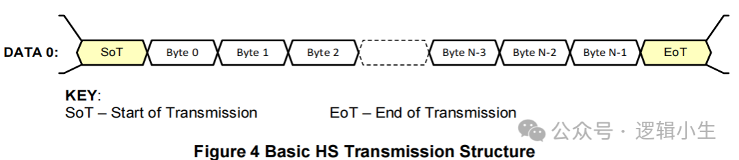
D-PHY low-level protocol specifies a minimum data unit of one byte, and that a transmission contains an integer number of bytes when using a forwarded clock; when using an embedded clock, each lane contains an integer number of symbols.
5.1.1 D-PHY Data Flow Control
There is no handshake between the Protocol and PHY layers that permit the Protocol layer to throttle data transfer to, or from, the PHY layer once transmission is underway. Packets shall be sent and received in their entirety and without interruption. The Protocol layer and data buffering on both ends of the Link shall always have bandwidth equal to, or greater than, PHY layer circuitry. A practical consequence is that the system implementer should ensure that receivers have bandwidth capability that is equal to, or greater than, that of the transmitter.
5.1.2 D-PHY Bidirectionality and Low Power Signaling Policy
In a Command Mode system, Data Lane 0 shall be bidirectional; additional Data Lanes shall be unidirectional. In a Video Mode system, Data Lane 0 may be bidirectional or unidirectional; additional Data Lanes shall be unidirectional. See Section 5.1.3 and Section 5.1.4 for details.
For both interface types, the Clock Lane shall be driven by the Host Processor only, never by the peripheral. Forward Direction [MIPI06] Low Power Transmissions (for clarity, DSI data) shall use Data Lane 0 only. Reverse Direction [MIPI06] Transmissions on Data Lane 0 shall use Low Power Mode only. The peripheral shall be capable of receiving any transmission in Low Power or High Speed Mode. Note that transmission bandwidth is substantially reduced when transmitting in LP mode.
For bidirectional lanes, data shall be transmitted in the peripheral-to-processor, or reverse, direction using Low-Power (LP) Mode only. See [MIPI06] for details on the different modes of transmission.
The interface between PHY and Protocol layers has several signals controlling bus direction. When a host transmitter requires a response from a peripheral, e.g., returning READ data or status information, it asserts TurnRequest to its PHY during the last packet of the transmission. This tells the PHY layer to assert the Bus Turn-Around (BTA) command following the EoT sequence.
When a peripheral receives the Bus Turn-Around command, its PHY layer asserts TurnRequest as an input to the Protocol layer. This tells the receiving Protocol layer that it shall prepare to send a response to the Host Processor. Normally, the packet just received tells the Protocol layer what information to send once the bus is available for transmitting to the Host Processor. After transmitting its response, the peripheral similarly hands bus control back to the Host Processor using a TurnRequest to its own PHY layer.
5.1.3 D-PHY Command Mode Interfaces
The minimum physical layer requirement [MIPI06] for a DSI Host Processor operating in Command Mode with a forwarded clock Lane is:
- Data Lane Module: CIL-MFAA (HS-TX, LP-TX, LP-RX, and LP-CD)
- Clock Lane Module: CIL-MCNN (HS-TX, LP-TX)
The minimum physical layer requirement [MIPI06] for a DSI peripheral operating in Command Mode with a forwarded clock Lane is:
- Data Lane Module: CIL-SFAA (HS-RX, LP-RX, LP-TX, and LP-CD)
- Clock Lane Module: CIL-SCNN (HS-RX, LP-RX)
The minimum physical layer requirement [MIPI06] for a DSI Host Processor operating in Command Mode with an embedded clock is:
- Data Lane Module: CIL-MFAA (HS-TX, LP-TX, LP-RX, and LP-CD)
The minimum physical layer requirement [MIPI06] for a DSI peripheral operating in Command Mode with an embedded clock is:
- Data Lane Module: CIL-SFAA (HS-RX, LP-RX, LP-TX, and LP-CD)
A Bidirectional Link shall support Reverse-Direction Escape Mode for Data Lane 0 to support LPDT for read data as well as ACK and TE Trigger Messages issued by the peripheral. In the Forward Direction, Data Lane 0 shall support LPDT as described in [MIPI06]. All Trigger messages shall be communicated across Data Lane 0.
5.1.4 D-PHY Video Mode Interfaces
The minimum physical layer requirement [MIPI06] for a DSI transmitter operating in Video Mode with a forwarded clock lane is:
- Data Lane Module: CIL-MFAN (HS-TX, LP-TX)
- Clock Lane Module: CIL-MCNN (HS-TX, LP-TX)
The minimum physical layer requirement [MIPI06] for a DSI receiver operating in Video Mode with a forwarded clock lane is:
- Data Lane Module: CIL-SFAN (HS-RX, LP-RX)
- Clock Lane Module: CIL-SCNN (HS-RX, LP-RX)
In the Forward Direction, Data Lane 0 shall support LPDT as described in [MIPI06]. All Trigger messages shall be communicated across Data Lane 0.
The minimum physical layer requirement [MIPI06] for a DSI transmitter operating in Video Mode with an embedded clock is:
- Data Lane Module: CIL-MFAN (HS-TX, LP-TX)
The minimum physical layer requirement [MIPI06] for a DSI receiver operating in Video Mode with an embedded clock is:
- Data Lane Module: CIL-SFAN (HS-RX, LP-RX)
In the Forward Direction, Data Lane 0 shall support LPDT as described in [MIPI06] or [MIPI12]. All Trigger messages shall be communicated across Data Lane 0.
5.1.5 D-PHY Bidirectional Control Mechanism
Turning the bus around is controlled by a token-passing mechanism: the Host Processor sends a Bus Turn-Around (BTA) request, which conveys to the peripheral its intention to release, or stop driving, the data path after which the peripheral can transmit one or more packets back to the Host Processor. When it is finished, the peripheral shall return control of the bus back to the Host Processor. Bus Turn-Around is signaled using an Escape Mode mechanism provided by PHY-level protocol.
In bidirectional systems, there is a remote chance of erroneous behavior due to EMI that could result in bus contention. Mechanisms are provided in this Specification for recovering from any bus contention event without forcing “hard reset” of the entire system.
5.1.6 D-PHY Clock Management
DSI Clock is a signal from the Host Processor to the peripheral. In some systems, it may serve multiple functions:
DSI Bit Clock: Across the Link, DSI Clock is used as the source-synchronous forwarded bit clock for capturing serial data bits in the receiver PHY. This clock shall be active while data is being transferred.
If embedded in a data Lane or data Lanes, then each DSI Clock is a pleisiosynchronous bit clock extracted by a clock recovery block in each receiver for capturing serial data bits in the receiver PHY. This clock shall be active while data is being transferred.
Byte Clock: Divided down, DSI Clock is used to generate a byte clock at the conceptual interface between the Protocol and Application layers. During HS Transmission, each byte of data is accompanied by a byte clock. Like the DSI Bit Clock, the byte clock shall be active while data is being transferred. At the Protocol layer to Application layer interface, all actions are synchronized to the byte clock.
Application Clock(s): Divided-down versions of DSI Bit Clock may be used for other clocked functions at the peripheral. These “application clocks” may need to run at times when no serial data is being transferred, or they may need to run constantly (continuous clock) to support active circuitry at the peripheral. Details of how such additional clocks are generated and used are beyond the scope of this document.
For continuous clock behavior, the Clock Lane remains in high-speed mode generating active clock signals between HS data packet Transmissions. For non-continuous clock behavior, the Clock Lane enters the LP-11 state between HS data packet Transmissions.
5.1.6.1 D-PHY Clock Requirements
All DSI transmitters and receivers using a physical layer Forwarded Clock feature shall support continuous clock behavior on the Clock Lane, and optionally may support non-continuous clock behavior. A DSI Host Processor shall support continuous clock for systems that require it, as well as having the capability of shutting down the serial clock to reduce power. Employing D-PHY 3.5 [MIPI06] with its Embedded Clock feature exempts transmitters and receivers from the continuous clocking requirement.
The physical layer [MIPI06] contains the ability to de-skew clock-to-Lane timing. The de-skew function does not apply for an embedded clock system. Physical layer de-skewing shall be performed in a manner that does not interfere with any display data, as follows:
1. Initial de-skew shall be completed prior to the Transmission of DSI packets.
2. Periodic de-skew shall support continuous clock mode operation.
3. Periodic de-skew shall be contained within any one video mode line, and shall meet these additional requirements to support video mode timing defined in Section 8.11:
- Periodic de-skew shall occur in a video back porch line or a video mode front porch line.
- Periodic de-skew shall not overlap any timing characters in the line, HSA, HSS, HSE, VSS, and VSE.
4. The DSI Transmitter shall not initiate a de-skew operation during the time between when the DSI Transmitter has asserted a TurnRequest and when the host has regained bus control.
In addition, a de-skew operation should not overlap an out-of-band TE event from the DSI receiver, and a de-skew operation should not be initiated until triggered by a TE event, either in-band or out-of-band.
Note that the Host Processor controls the desired mode of clock operation. Host protocol and applications control Clock Lane operating mode (High Speed or Low Power mode). System designers are responsible for understanding the clock requirements for peripherals attached to DSI, and for controlling clock behavior in accordance with those requirements.
In low power signaling mode, LP clock is functionally embedded in the data signals. When LP data transmission ends, the clock effectively stops and subsequent LP clocks are not available to the peripheral. The peripheral shall not require additional bits, bytes, or packets from the Host Processor in order to complete processing or pipeline movement of received data in LP mode transmissions. There are a variety of ways to meet this requirement. For example, the peripheral may generate its own clock, or it may require the Host Processor to keep the HS serial clock running.
The handshake process for BTA allows only limited mismatch of Escape Mode clock frequencies between a Host Processor and a peripheral. The Escape Mode frequency ratio between Host Processor and peripheral shall not exceed 3:2. The Host Processor is responsible for controlling its own clock frequency to match the peripheral. The Host Processor LP clock frequency shall be in the range of 67% to 150% of peripheral LP clock frequency. Therefore, the peripheral implementer shall specify a peripheral’s nominal LP clock frequency and the guaranteed accuracy.
5.1.6.2 D-PHY Clock Power and Timing
Additional timing requirements in [MIPI06] specify the timing relationship between the power state of data signal(s) and the power state of the clock signal. It is the responsibility of the Host Processor to observe this timing relationship. If the DSI Clock runs continuously, these timing requirements do not apply.
5.1.7 D-PHY System Power-Up and Initialization
System power-up is a multi-state process that depends not only on initialization of the host (Host Processor) and client (peripheral) devices, but also possibly on internal delays within the client device. This Section specifies the parameters necessary for operation and makes several recommendations to help ensure the system power-up process is robust.
After power-up, the Host Processor shall observe an initialization period, TINIT, during which it shall drive a sustained TX-Stop state (LP-11) on all Lanes of the Link. See [MIPI06] for descriptions of TINIT and the TX-Stop state.
Peripherals shall power up in the RX-Stop state and monitor the Link to determine if the Host Processor has asserted a TX-Stop state for at least the TINIT period. The peripheral shall ignore all Link states prior to detection of a TINIT event. The peripheral shall be ready to accept bus transactions immediately following the end of the TINIT period.
Detecting the TINIT event requires some minimal timing capability on the peripheral. However, accuracy is not critical as long as a TINIT event can be reliably detected; an R-C timer with ±30% accuracy is acceptable in most cases.
If the peripheral requires a longer period after power-up than the TINIT period driven by the Host Processor, this requirement shall be declared in peripheral product information or data sheets. The Host Processor shall observe the required additional time after peripheral power-up.
Figure 5 illustrates an example power-up sequence for a DSI display module. In the figure, a power-on reset (POR) mechanism is assumed for initialization. Internally within the display module, de-assertion of POR could happen after both I/O and core voltages are stable. The worst case tPOR parameter can be defined by the display module data sheet. tINIT_CLIENT represents the minimum initialization period (TINIT) defined in [MIPI06] for a host driving LP-11 to the display. This interval starts immediately after the tPOR period. The peripheral might need an additional tINTERNAL_DELAY time to reach a functional state after power-up. In this case, tINTERNAL_DELAY should also be defined in the display module data sheet. In this example, the host’s tINIT_HOST parameter is programmed for driving LP-11 for a period longer than the sum of tINIT_CLIENT and tINTERNAL_DELAY. The display module ignores all Lane activities during this time.
5.2 DSI Physical Layer for C Option
This Section provides a brief overview of the C Option physical layer used in DSI. See [MIPI07] for more details.
Information is transferred between Host Processor and peripheral using one or more serial data signals. The action of sending high-speed serial data across the bus is called an HS Transmission or burst.
Between Transmissions, the differential data signal or Lane goes to a Low-Power State (LPS). Interfaces should be in LPS when they are not actively transmitting or receiving high-speed data.
The C-PHY low-level protocol specifies a minimum data unit of two bytes, and a Transmission contains an even number of bytes.
C-PHY converts 2 bytes to 7 symbol transitions. Data is distributed with a granularity of 2 bytes. Every pair of bytes constructs a 16-bit word with most significant byte as the higher 8 bits, and the least significant byte as the lower 8 bits, i.e., { Byte (2n+1), Byte (2n) }, where Byte (2n+1) is the most significant byte of the 16-bit word sent to the symbol mapper.
Filler Bytes have a value of “0” and are used to convert a lone byte to a 16-bit word. At the end of a packet, if there is no actual data byte available to be paired with a given “Byte (2n)”, then Byte (2n) is converted to a 16-bit word by padding a Filler Byte of “0” in place of “Byte (2n+1)”, prior to the symbol mapping.
5.2.1 C-PHY Data Flow Control
There is no handshake between the Protocol and PHY layers that permit the Protocol layer to throttle data transfer to, or from, the PHY layer once Transmission is underway. Packets shall be sent and received in their entirety and without interruption. The Protocol layer and data buffering on both ends of the Link shall always have bandwidth equal to, or greater than, PHY layer circuitry. A practical consequence is that the system implementer should ensure that receivers have bandwidth capability that is equal to, or greater than, that of the transmitter.
5.2.2 C-PHY Bidirectionality and Low Power Signaling Policy
The physical layer for a DSI implementation is composed of one to four Data Lanes. In a Command Mode system, Data Lane 0 shall be bidirectional; additional Data Lanes shall be unidirectional. In a Video Mode system, Data Lane 0 may be bidirectional or unidirectional; additional Data Lanes shall be unidirectional.
See Section 5.2.3 and Section 5.2.4 for details.
Forward Direction Low Power Transmissions (for clarity, DSI data) shall use Data Lane 0 only. Reverse Direction Transmissions on Data Lane 0 shall use Low Power Mode only. The peripheral shall be capable of receiving any Transmission in Low Power or High-Speed Mode. Note that Transmission bandwidth is substantially reduced when transmitting in LP mode.
For bidirectional Lanes, data shall be transmitted in the peripheral-to-processor, or reverse, direction using Low-Power (LP) Mode only. See [MIPI07] for details on the different modes of Transmission.
The interface between PHY and Protocol layers has several signals controlling bus direction. When a host transmitter requires a response from a peripheral, e.g., returning READ data or status information, it asserts TurnRequest to its PHY during the last packet of the Transmission. This tells the PHY layer to assert the Bus Turn-Around (BTA) command following the EoT sequence.
When a peripheral receives the Bus Turn-Around command, its PHY layer asserts TurnRequest as an input to the Protocol layer. This tells the receiving Protocol layer that it shall prepare to send a response to the Host Processor. Normally, the packet just received tells the Protocol layer what information to send once the bus is available for transmitting to the Host Processor.
After transmitting its response, the peripheral similarly hands bus control back to the Host Processor using a TurnRequest to its own PHY layer.
5.2.3 C-PHY Command Mode Interfaces
The minimum physical layer requirement [MIPI07] for a DSI Host Processor operating in Command Mode is:
- Data Lane Module: CIL-MFAA (HS-TX, LP-TX, LP-RX, and LP-CD)
The minimum physical layer requirement [MIPI07] for a DSI peripheral operating in Command Mode is:
- Data Lane Module: CIL-SFAA (HS-RX, LP-RX, LP-TX, and LP-CD)
A Bidirectional Link shall support Reverse-Direction Escape Mode for Data Lane 0 to support LPDT for read data as well as ACK and TE Trigger Messages issued by the peripheral. In the Forward Direction, Data Lane 0 shall support LPDT as described in [MIPI07]. All Trigger messages shall be communicated across Data Lane 0.
5.2.4 C-PHY Video Mode Interfaces
The minimum physical layer requirement [MIPI07] for a DSI transmitter operating in Video Mode is:
- Data Lane Module: CIL-MFAN (HS-TX, LP-TX)
The minimum physical layer requirement [MIPI07] for a DSI receiver operating in Video Mode is:
- Data Lane Module: CIL-SFAN (HS-RX, LP-RX)
In the Forward Direction, Data Lane 0 shall support LPDT as described in [MIPI07]. All Trigger messages shall be communicated across Data Lane 0.
5.2.5 C-PHY Bidirectional Control Mechanism
Turning the bus around is controlled by a token-passing mechanism: the Host Processor sends a Bus Turn-Around (BTA) request, which conveys to the peripheral its intention to release, or stop driving, the data path after which the peripheral can transmit one or more packets back to the Host Processor. When it is finished, the peripheral shall return control of the bus back to the Host Processor. Bus Turn-Around is signaled using an Escape Mode mechanism provided by PHY-level protocol.
In bidirectional systems, there is a remote chance of erroneous behavior due to EMI that could result in bus contention. Mechanisms are provided in this Specification for recovering from any bus contention event without forcing “hard reset” of the entire system.
5.2.6 C-PHY Clock Management
C-PHY embeds the clock in the high-speed signal sent over each of the Lanes. The high-speed signal clock is conveyed from the Host Processor to the peripheral. In some systems, the high-speed signal clock may serve multiple functions:
Word Clock (Informative): Divided down, the high-speed signal clock is used to generate a word clock at the conceptual interface between the Protocol and Application layers. During HS Transmission, every 2 bytes of data is accompanied by the associated word clock. Like the high-speed signal clock, the word clock will be active while data is being transferred. At the Protocol layer to Application layer interface, all actions can be synchronized to the word clock. The word clock is exactly 1/7 of the High-Speed symbol rate.
Application Clock(s) (Informative): Divided-down versions of high-speed signal clock may be used for other clocked functions at the peripheral. These “application clocks” may need to run at times when no serial data is being transferred, or they may need to run constantly (continuous clock) to support active circuitry at the peripheral. Details of how such additional clocks are generated and used are beyond the scope of this document.
All of the Lanes should enter the LP-111 state between HS data packet Transmissions. Continuous clock behavior is optional and is out of scope of this specification.
5.2.6.1 C-PHY Clock Requirements
Note that in Low Power signaling mode, LP clock is functionally embedded in the data signals. When LP data Transmission ends, the clock effectively stops, and subsequent LP clocks are not available to the peripheral. The peripheral shall not require additional bits, bytes, or packets from the Host Processor in order to complete processing or pipeline movement of received data in LP mode transmissions. There are a variety of ways to meet this requirement. For example, the peripheral may generate its own clock, or it may require the Host Processor to keep the HS serial clock running.
The handshake process for BTA allows only limited mismatch of Escape Mode clock frequencies between a Host Processor and a peripheral. The Escape Mode frequency ratio between Host Processor and peripheral shall not exceed 3:2. The Host Processor is responsible for controlling its own clock frequency to match the peripheral. The Host Processor LP clock frequency shall be in the range of 67% to 150% of peripheral LP clock frequency. Therefore, the peripheral implementer shall specify a peripheral’s nominal LP clock frequency and the guaranteed accuracy.
5.2.7 C-PHY System Power-Up and Initialization
System power-up is a multi-state process that depends not only on initialization of the host (Host Processor) and client (peripheral) devices, but also possibly on internal delays within the client device. This Section specifies the parameters necessary for operation and makes several recommendations to help ensure the system power-up process is robust.
After power-up, the Host Processor shall observe an initialization period, TINIT, during which it shall drive a sustained TX-Stop state (LP-111) on all Lanes of the Link. See [MIPI07] for descriptions of TINIT and the TX-Stop state.
Peripherals shall power up in the RX-Stop state and monitor the Link to determine if the Host Processor has asserted a TX-Stop state for at least the TINIT period. The peripheral shall ignore all Link states prior to detection of a TINIT event. The peripheral shall be ready to accept bus transactions immediately following the end of the TINIT period.
Detecting the TINIT event requires some minimal timing capability on the peripheral. However, accuracy is not critical as long as a TINIT event can be reliably detected; an R-C timer with ±30% accuracy is acceptable in most cases.
If the peripheral requires a longer period after power-up than the TINIT period driven by the Host Processor, this requirement shall be declared in peripheral product information or data sheets. The Host Processor shall observe the required additional time after peripheral power-up.
Figure 6 illustrates an example power-up sequence for a DSI display module. In the figure, a power-on reset (POR) mechanism is assumed for initialization. Internally within the display module, de-assertion of POR could happen after both I/O and core voltages are stable. The worst case tPOR parameter can be defined by the display module data sheet. tINIT_CLIENT represents the minimum initialization period (TINIT) defined in [MIPI07] for a host driving LP-111 to the display. This interval starts immediately after the tPOR period. The peripheral might need an additional tINTERNAL_DELAY time to reach a functional state after power-up. In this case, tINTERNAL_DELAY should also be defined in the display module data sheet. In this example, the host’s tINIT_HOST parameter is programmed for driving LP-111 for a period longer than the sum of tINIT_CLIENT and tINTERNAL_DELAY. The display module ignores all Lane activities during this time.
5.3 Allowed Physical Layers in DSI-2
This Specification supports only the two physical layer options described in Sections 5.1 and 5.2. One of the physical layers, D-PHY or C-PHY, or both, shall be used with DSI-2 and no others.
Manufacturers of devices employing DSI-2 shall specify whether C Option, D Option, or both are supported in the manufacturer’s supporting documentation, such as a data sheet.
At the time of this document’s publication, MIPI’s Display Working Group considered D-PHY v2.1 to be compatible with the earlier D-PHY v1.2.
At the time of this document’s publication, provisions of D-PHY 3.5 [MIPI06] should be compatible with the earlier D-PHY v2.1 and D-PHY v1.2. Some optional features of D-PHY versions not included in this specification and not necessarily limited to this list are: ALP (Alternative Low Power) modes, hi-speed reverse mode, or hi-speed idle.
At the time of this document’s publication, MIPI’s Display Working Group considered C-PHY 2.1 [MIPI07] to be compatible with the earlier v1.2 of C-PHY.
In addition to the physical layer connections noted above in this section (i.e., Section 5.3), DSI-2 may connect to other referenced physical layers via Protocol Adaptation Layers (PALs). At the time of this publication, only the following PAL is authorized:
- MIPI Alliance A-PHY Protocol Adaptation Layer Specification for DSI-2 (MIPI PAL/DSI-2) [MIPI09].