The global semiconductor industry has entered a super cycle.
China-U.S. technology friction.
China’s integrated circuit industry support policies are strengthening, etc.
Multiple factors overlap.
The outlook for the chip industry is promising.
First, let’s clarify the concepts and differences between “semiconductor,” “chip,” and “integrated circuit”, in general, semiconductor, integrated circuit, and chip can be considered equivalent because they refer to essentially the same thing.
A semiconductor is a type of material, and since the proportion of integrated circuits on semiconductor substrates is very high, exceeding 80%, the industry habitually refers to the semiconductor industry as the integrated circuit industry.The chip is the carrier of the integrated circuit, and broadly speaking, we equate the chip with the integrated circuit.
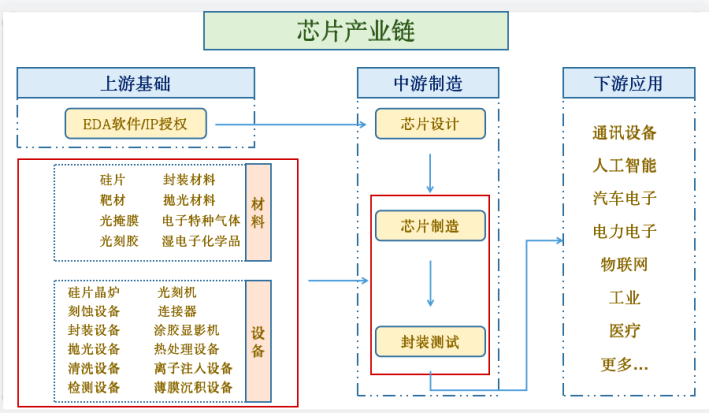
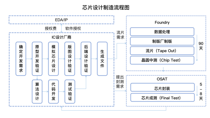
Chip Industry Supply Chain
With the increasing importance placed on integrated circuits in our country, the EDA/IP licensing industry is entering a rapid development phase,the EDA/IP supply chain is mainly divided into two levels,the basic layer and the application layer.
The basic layer refers to EDA/IP providers, mainly divided intoEDA tools and IP cores..
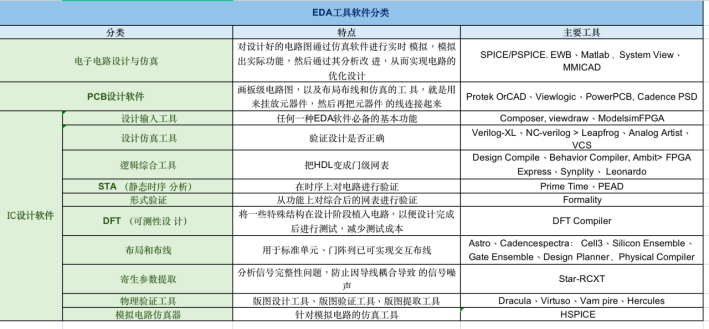
EDA is the most upstream and high-end industry in the integrated circuit supply chain. EDA stands for Electronic Design Automation, which has developed from the concepts of Computer-Aided Design (CAD), Computer-Aided Manufacturing (CAM), Computer-Aided Testing (CAT), and Computer-Aided Engineering (CAE). EDA tools are the platforms for chip design.
EDA is a broad form of CAD, a specialized industry software.EDA software design incorporates extensive knowledge from mathematics, graph theory, physics, materials, processes, etc., to achieve automatic design of electronic products.
EDA tools are automated software tools required for chip design. Using EDA tools, the entire process of circuit design, performance analysis, and IC layout design can be completed automatically by computers. With EDA tools, electronic designers can also start designing electronic systems from concepts, algorithms, protocols, etc., completing the entire process from circuit design, performance analysis to designing IC layouts or PCB layouts. After decades of development, EDA tools are also very rich and can be categorized by function and usage scenarios into circuit design and simulation tools, PCB design software, IC design software, PLD design tools, etc.
IP cores (Intellectual Property Cores) are hardware description language programs with specific circuit functions. They refer to design modules in integrated circuit design that are verifiable, reusable, have a certain defined function, and possess independent intellectual property rights, which are independent of chip manufacturing processes and can be ported to different integrated circuit processes.
First, enterprise application services, mainly involve integrated circuit design companies, manufacturing companies, packaging and testing companies, and IC design service companies purchasing EDA tools and IP cores for integrated circuit design, manufacturing, and packaging testing;
Second, government application services, mainly refer to public service platforms established by the government; third, scientific research application services, mainly involve universities, research institutions, training centers, and some joint laboratories purchasing EDA/IP for teaching, scientific research, and training.
The core competitiveness of chips is a key indicator of measuring a country’s information technology development level, with chip design occupying a crucial position.The focus of TMT industry development on 5G chips and AI chips is also centered on chip design, which cannot be separated from chip design software EDA, making it a critical part of the chip supply chain. The core strength of chips also lies in chip design, which has made rapid progress domestically, and there is great potential in this field for the future.
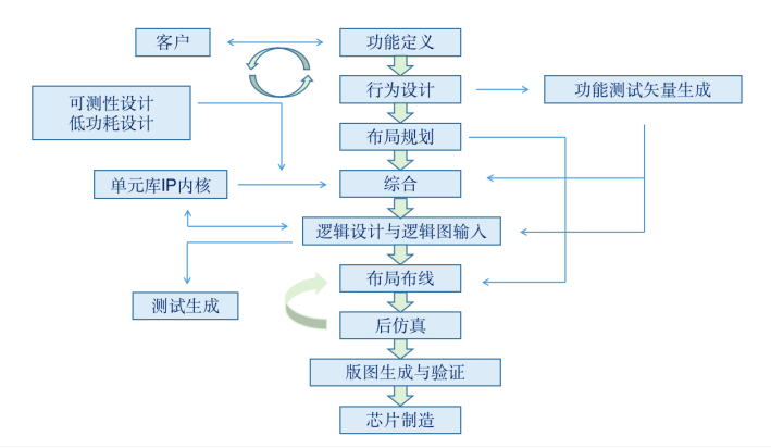
The chip design process can be roughly divided into determining project requirements, system-level design, logic design, and hardware design.In the IC design industry, a few giant companies dominate, with the U.S. IC design industry being in a leading position.
Chip design can be divided into front-end and back-end; the front-end is mainly responsible for logic implementation, while the back-end is closely integrated with the process.Front-end technology mainly converts HDL design coding into netlist gate-level netlists and performs a series of simulations and verifications to ensure the gate-level circuit diagram meets specifications, timing, and functionality requirements;the back-end primarily involves layout and routing of gate-level circuit diagrams, generating layouts, while verifying signal integrity, layout compliance, and process requirements.
Chip Industry Business Models
Currently, the main business models for chips can be divided into two categories: IDM (Integrated Device Manufacturer) model and vertical division of labor model.
IDM (Integrated Device Manufacture) Model:
Semiconductor companies that handle everything from design to manufacturing, packaging, and selling their own brand ICs are called IDM companies.International IDM representatives include:Intel, SK Hynix, Micron, NXP, Infineon, Sony, Texas Instruments (TI), Samsung, Toshiba, STMicroelectronics, etc.IDM manufacturers mainly include:China Resources Microelectronics, Silan Microelectronics, Yangjie Technology, Suzhou Goodix, Shanghai Belling, etc.
Vertical Division of Labor Model:
Some semiconductor companies only do IC design and do not have chip fabrication plants (Fabs), which are typically referred to as Fabless, such as Huawei, ARM, NVIDIA, and Qualcomm. Additionally, some companies only do foundry work and do not engage in design, known as foundries;representative companies include TSMC, GlobalFoundries, SMIC, and UMC.
Based on the above two business models, existing semiconductor companies can be divided into IDM, Foundry, Fabless, and Fab-lite (a hybrid between IDM and Fabless).
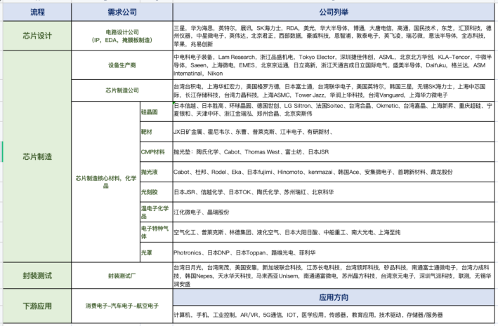
Examples of Companies in the Chip Industry:
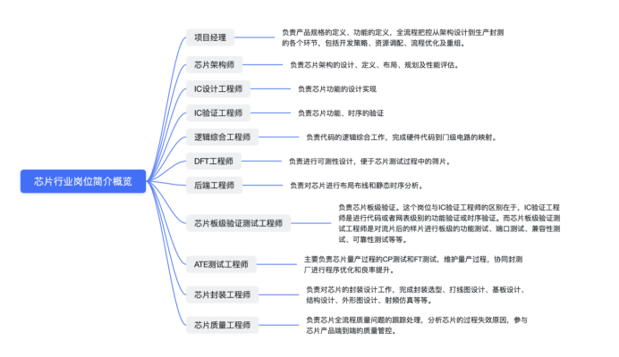
Chip Industry Job Positions
| Project Manager: Responsible for defining product specifications and functions, overseeing the entire process from architectural design to production and testing, including development strategies, resource allocation, process optimization, and restructuring.
| Chip Architect: Responsible for the design, definition, layout, planning, and performance evaluation of chip architecture.
| IC Design Engineer: Responsible for the design and implementation of chip functions.
| IC Verification Engineer: Responsible for verifying chip functions and timing.
| Logic Synthesis Engineer: Responsible for the logical synthesis of code, mapping hardware code to gate-level circuits.
| DFT Engineer: Responsible for designing testability to facilitate chip testing.
| Back-End Engineer: Responsible for layout and routing of chips and static timing analysis.
| Chip Board-Level Validation Test Engineer: Responsible for board-level validation of chips. This position differs from the IC verification engineer, who conducts functional or timing verification at the code or netlist level, while the chip board-level validation test engineer tests the functionality, port compatibility, reliability, etc. of samples after tape-out.
| ATE Test Engineer: Mainly responsible for CP testing and FT testing during the chip mass production process, maintaining the production process, and collaborating with packaging and testing factories for program optimization and yield improvement.
| Chip Packaging Engineer: Responsible for packaging design work for chips, completing packaging selection, wire bonding design, substrate design, structural design, appearance design, RF simulation, etc.
| Chip Quality Engineer: Responsible for tracking and handling quality issues throughout the chip process, analyzing the causes of process failures, and participating in end-to-end quality control of chip products.
Chip Industry Job Directions
Chip design (IC Design) is divided into two directions:digital and analog.
Job description: Determine the feasibility and performance of the chip’s system functions and specifications. Divide the chip into software and hardware, design chip architecture schemes, define chip specs, build top-level architecture and modeling, high-level simulation.
Senior position, with extensive experience in the entire process and multiple successful tape-out experiences. Salaries in the millions are common, but the requirements are also high.
10+ years of experience in the IC industry, having grown from other design engineers, with an emphasis on experience, accumulation, and talent. The possibility of design engineers becoming architects is greater.
Job description: Based on specs, use hardware description language, Verilog HDL to complete the RTL design of each module.
Familiar with logic design, familiar with digital chip IP modules, proficient in Verilog HDL.
Newcomers with relevant majors are needed, starting from simple auxiliary work and modules, especially suitable for those strong in mathematics, algorithms, and logic.
Job description: Build the verification environment, design test vectors, and collect verification coverage to ensure RTL design meets specs.
Familiar with verification tools, able to use SV and UVM to build verification environments, write test cases, and proficient in software programming.
Newcomer friendly, with low requirements for knowledge of chip internal structure and underlying knowledge, easy to get started, suitable for software-oriented individuals skilled in programming.
Job description: Generate gate-level netlists from RTL synthesis, layout and route, perform timing analysis, DRC/LVS, while reducing area and power consumption based on requirements.
Familiar with back-end design tools; there are many tools for back-end use, familiar with layouts, and understand chip manufacturing processes.
Hiring newcomers, starting from auxiliary work and simple modules.
While designing the chip, testing circuits need to be added, incorporating DFT design modules, and inserting scan chains to improve test coverage and reduce chip testing time.
Familiar with DFT principles, processes, and relevant EDA tools.
Some experience in digital chip design is required; less newcomer friendly.
Analog Direction: Analog is further divided into analog design and analog layout
Construct various modules of analog circuits according to spec requirements using simulation tools.
Requirements: Familiar with analog circuit principles, circuit unit structures, semiconductor devices and processes, proficient in relevant EDA tools.
The minimum requirement is relevant majors for newcomers, starting from auxiliary work and simple modules, especially suitable for those familiar with electronics, electrical engineering, instrumentation, automation, etc.
2. Layout Designer/Engineer
Draw layouts based on the circuit design drawings completed by designers.
Newcomer friendly, low comprehensive knowledge requirements, familiar with circuits, mastering tools, and easy to get started with no special professional background required.
Overall, every position for chip engineers is very promising, with relatively high salary levels. Among them, chip architecture is at the top with annual salaries in the million range, generally requiring extensive work experience and familiarity with various stages of the chip design process, along with successful tape-out experiences!
Next is design, which tests logical thinking and is generally more challenging. As for verification, back-end, DFT, and other positions, the development prospects are still good, with salary levels for campus recruitment and social recruitment being basically the same. Analog layout is relatively simpler, and salaries are generally lower than the previous positions, but the market demand is higher!
Characteristics and Advantages of Working in the Chip Industry
Characteristics of Working in the Chip Industry
1. High Learning Difficulty:
Learning about chips is indeed quite difficult, as it requires understanding the basics of physics, digital electronics, programming, etc. Chip development deals with pure logical development, and indeed the enjoyment is less than that of software development and the internet.
In previous years, chip salaries were far lower than those in the internet sector, but in recent years they have reached similar levels. Moreover, there are relatively few good chip companies in China. Companies like Huawei and Unisoc offer better compensation.
3. Strong Professionalism:
Chip development involves highly specialized knowledge, and is primarily used within the industry, making it non-transferable to other fields. If one transitions to another field, previous accumulations may become obsolete.
4. Limited Promotion Space:
The promotion path in chips is solely technical; once a technician, always a technician, with very few opportunities to transition into product, sales, or management roles. Working in technology can be mentally taxing, as one will notice that engineers in this field tend to have darker circles under their eyes and thinning hair, with limited social interactions outside of their work.
Advantages of Working in the Chip Industry:
1. The chip industry is a sunrise industry in China; many research institutes, universities, and enterprises have established chip departments, increasing job opportunities. Furthermore, companies engaged in chips generally have strong backgrounds and ample funding.
2. The entry barrier for chips is relatively high, facing less pressure for replaceability. Essentially, if you establish yourself in the chip field, you won’t be easily replaced by newcomers, unlike other industries that face mid-life crises.
3.Both the national and local governments have introduced policies favorable to chip development, which also increases the attention and returns for those working in the industry.
Relevant Majors for Entering the Chip Industry include Microelectronics Science and Engineering Materials, Electrical and Electronic Engineering, Optics, Chemistry, Mathematics, Physics, Mechanical Engineering, Automation, Computer Science, Industrial Engineering, etc.

Job Seeking, Internships, Career Planning
Feel free to add me on WeChat for inquiries~
Add the team leader’s WeChat
WeChat ID: Canadaliuxuezhongxin

Want to conquer the job market?
Welcome to click the mini program below
For more study abroad consulting, please follow “Canada Study Center”
New and reliable content is waiting for you every day!
Copyright statement: Most images and content are sourced from the internet, copyright belongs to the author. If there are any infringements, please contact us for resolution.