
When it comes to PCB boards, many friends might think of how ubiquitous they are around us, from all household appliances, various components inside computers, to various digital products; almost every electronic product will use PCB boards. So what exactly is a PCB board? A PCB board is a Printed Circuit Board, which serves as a substrate for electronic components to be inserted, with wiring. By using printing methods to apply anti-corrosive lines on a copper-plated substrate, the lines are then etched and washed out.
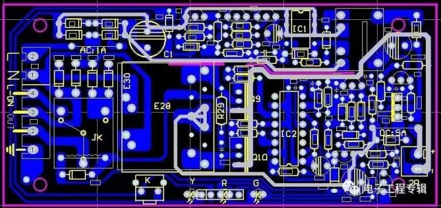
PCB boards can be divided into single-layer boards, double-layer boards, and multi-layer boards. Various electronic components are integrated onto the PCB board. In the simplest single-layer PCB, components are concentrated on one side, while the wires are concentrated on the other side. This requires holes to be drilled on the board, allowing the component pins to pass through to the other side, which is why the component pins are soldered on the opposite side. Therefore, the front and back sides of such a PCB are referred to as the Component Side and the Solder Side, respectively. A double-layer board can be seen as two single-layer boards glued together, with electronic components and wiring on both sides. Sometimes, it’s necessary to connect a single wire from one side to the other, which is achieved through vias. Vias are small holes filled or coated with metal on the PCB, connecting the wires on both sides. Nowadays, many computer motherboards use 4-layer or even 6-layer PCBs, while graphics cards typically use 6-layer PCBs. Many high-end graphics cards, such as the nVIDIA GeForce 4 Ti series, use 8-layer PCBs, which are known as multi-layer PCBs. In multi-layer PCBs, there are also challenges with connecting the lines between various layers, which can also be accomplished through vias. Since they are multi-layer PCBs, sometimes the vias do not need to penetrate the entire PCB; these vias are called buried vias and blind vias, as they only penetrate a few layers. Blind vias connect several internal PCBs to the surface PCB without penetrating the entire board. Buried vias only connect internal PCBs, making them invisible from the surface. In multi-layer PCBs, each layer is directly connected to the ground and power lines. Therefore, we categorize the layers as Signal layers, Power layers, or Ground layers. If components on the PCB require different power supplies, these types of PCBs typically have two or more power and wiring layers. The more layers a PCB has, the higher the cost. Of course, using more layers of PCB is helpful for providing signal stability.The professional PCB manufacturing process is quite complex; for instance, a 4-layer PCB is mostly used in motherboards. During manufacturing, the two middle layers are pressed, cut, etched, and oxidized before being plated. These four layers are the component layer, power layer, ground layer, and solder mask layer. Then, these four layers are pressed together to form a PCB for the motherboard. After that, holes are drilled and vias are made. After cleaning, the lines on the outer two layers are printed, copper-plated, etched, tested, and coated with solder mask and silkscreen. Finally, the entire PCB (including many motherboard sections) is stamped into individual motherboard PCBs, which are then vacuum-packed after testing. If the copper plating is not done well during the PCB manufacturing process, there may be adhesion issues, leading to hidden short circuits or capacitive effects (which can easily cause interference). The vias on the PCB must also be taken into account. If the holes are not drilled in the center but are offset, it will result in uneven matching or potential contact with the middle power or ground layers, leading to potential short circuits or grounding issues.
Wiring Process of Copper LinesThe first step in production is to establish the wiring between components. We use negative photo transfer to display the working film on the metal conductor. This technique involves covering the entire surface with a thin layer of copper foil and eliminating the excess parts. The additive transfer is another less commonly used method, which only applies copper lines where needed, but we will not elaborate on that here. The positive photoresist is made from a photosensitive agent that dissolves under illumination. There are many ways to handle the photoresist on the copper surface, but the most common method is to heat it and roll it over the surface containing the photoresist. It can also be sprayed in liquid form, but dry film provides higher resolution and can produce finer lines. The mask is just a template for manufacturing the PCB layer. Before the photoresist on the PCB is exposed to UV light, the mask covering the top prevents some areas of the photoresist from being exposed. The areas covered by the photoresist will become wiring. After developing the photoresist, the other exposed copper parts need to be etched. The etching process can involve immersing the board in an etching solvent or spraying the solvent onto the board. Typically, trichloroethylene is used as the etching solvent. After etching, the remaining photoresist is removed.1. Wiring Width and CurrentGenerally, the width should not be less than 0.2mm (8mil).In high-density, high-precision PCBs, the spacing and line width are generally 0.3mm (12mil).When the copper foil thickness is around 50um, a wire width of 1-1.5mm (60mil) can handle 2A.The common ground is generally 80mil; for applications with microprocessors, more attention is needed.2. What Frequency is Considered High-Speed?When the rise/fall time of the signal is < 3-6 times the signal transmission time, it is considered high-speed.For digital circuits, the key is to look at the steepness of the signal edges, specifically the rise and fall times. According to a classic book, “High Speed Digital Design”, if the time for a signal to rise from 10% to 90% is less than 6 times the line delay, it is considered a high-speed signal! This means that even an 8KHz square wave signal, as long as the edges are steep enough, is still a high-speed signal. During wiring, transmission line theory needs to be applied.3. Stacking and Layering of PCB BoardsFour-layer boards have several stacking orders. Below are descriptions of the advantages and disadvantages of various stacking methods:First scenarioGNDS1+POWERS2+POWERGNDSecond scenarioSIG1GNDPOWERSIG2Third scenarioGNDS1S2POWERNote: S1 is the first signal wiring layer, S2 is the second signal wiring layer; GND is the ground layer, and POWER is the power layer.The first scenario is considered the best among four-layer boards. The outer layers are ground layers, providing shielding against EMI, while the power layer is very close to the ground layer, resulting in low internal resistance and achieving optimal results. However, this scenario cannot be used when the board density is relatively high. This is because the integrity of the first ground layer cannot be guaranteed, which can lead to worse signal quality on the second layer. Additionally, this structure cannot be used when the entire board has a relatively high power consumption.The second scenario is the most commonly used method. From the board’s structure, it is also not suitable for high-speed digital circuit design. This is because it is difficult to maintain low power resistance in this structure. For a board with a thickness of 2mm, the requirement is Z0=50 ohms, with a line width of 8mil and a copper foil thickness of 35μm. The distance between the signal layer and the ground layer is 0.14mm, while the distance between the ground layer and the power layer is 1.58mm, significantly increasing the internal resistance of the power supply. In this structure, since radiation is directed into space, a shielding plate is needed to reduce EMI.The third scenario has the best signal quality on the S1 layer, followed by S2. It provides shielding against EMI but has a larger power resistance. This board can be used in scenarios where the entire board has high power consumption or is a source of interference or is closely adjacent to interference sources.4. Impedance MatchingThe amplitude of the reflected voltage signal is determined by the source reflection coefficient ρs and the load reflection coefficient ρL.ρL = (RL – Z0) / (RL + Z0) and ρS = (RS – Z0) / (RS + Z0)In the above formula, if RL=Z0, then the load reflection coefficient ρL=0. If RS=Z0, then the source reflection coefficient ρS=0.Since the impedance Z0 of ordinary transmission lines typically meets the requirement of around 50Ω, while the load impedance usually ranges from several thousand ohms to tens of thousands of ohms, achieving impedance matching at the load end is relatively difficult. However, since the output impedance of the signal source (output) is usually small, roughly a few ohms, achieving impedance matching at the source end is much easier. If resistors are connected at the load end, they will absorb part of the signal, which is detrimental to transmission (in my understanding). When selecting the TTL/CMOS standard with a 24mA drive current, its output impedance is approximately 13Ω. If the transmission line impedance Z0=50Ω, then a 33Ω source matching resistor should be added. 13Ω + 33Ω = 46Ω (approximately 50Ω, weak underdamping helps the signal’s setup time).When selecting other transmission standards and drive currents, the matching impedance will vary. In high-speed logic and circuit design, for some critical signals, such as clock and control signals, we recommend adding source matching resistors.In this way, signals will also reflect back from the load end, and because of source end impedance matching, the reflected signal will not reflect back again.5. Power Line and Ground Line Layout ConsiderationsPower lines should be as short as possible, run in a straight line, and preferably in a tree-like structure, avoiding circular paths.Ground loop issues: For digital circuits, the ground loop current caused by ground loops is generally at the millivolt level, while the interference threshold for TTL is 1.2V, and CMOS circuits can reach half the power supply voltage, meaning that ground loop currents will not adversely affect circuit operation. Conversely, if the ground is not closed, the problem will be greater, as the pulse power current generated during the operation of digital circuits will cause imbalances in ground potential at various points. For instance, I measured that the ground current of a 74LS161 during inversion was 1.2A (measured with a 2Gsps oscilloscope, with a ground current pulse width of 7ns). Under the impact of large pulse currents, if a branched ground line (25mil width) is used, the potential difference between various points on the ground line can reach the hundred-millivolt level. However, by using a ground loop, the pulse current will spread to various points on the ground line, greatly reducing the likelihood of circuit interference. Using a closed ground line, I measured that the maximum instantaneous potential difference between devices in a closed ground line is about one-half to one-fifth of that in an open ground line. Of course, the measured data varies greatly among different density and speed circuit boards; what I mentioned above refers to a level comparable to the Z80 Demo board that comes with Protel 99SE. For low-frequency analog circuits, I believe that the power frequency interference sensed from space cannot be simulated or calculated in any way. If the ground is not closed, ground eddy currents will not be generated, and the theoretical basis for beckhamtao’s assertion that “the open ground will generate greater power frequency induced voltage” can be illustrated with two examples. Seven years ago, I took over someone else’s project, a precision pressure gauge using a 14-bit A/D converter, but the measured effective precision was only 11 bits. Upon investigation, I found that there was a 15mVp-p power frequency interference on the ground line. The solution was to break the analog ground loop of the PCB and use a branched distribution of the ground line from the front-end sensor to the A/D. The PCB of the production model was then produced according to the branched line layout, and no issues have occurred since. The second example involves a friend who loves audio and DIYed an amplifier, but there was always an AC hum. I suggested breaking the ground loop, and the problem was resolved. Afterward, this friend checked dozens of PCB diagrams of “Hi-Fi brands” and confirmed that none of them used ground loops in the analog section.6. Principles of PCB Design and Anti-Interference MeasuresPrinted Circuit Boards (PCBs) are the supporting components for circuit elements and devices in electronic products. They provide electrical connections between circuit elements and devices. With the rapid development of electrical technology, the density of PCBs is increasing. The quality of PCB design has a significant impact on anti-interference capabilities. Therefore, when designing PCBs, it is essential to adhere to general PCB design principles and comply with anti-interference design requirements.General Principles of PCB DesignTo ensure optimal performance of electronic circuits, the layout of components and wiring is crucial. To design high-quality and cost-effective PCBs, the following general principles should be followed:LayoutFirst, consider the size of the PCB. If the PCB is too large, the printed lines will be long, increasing impedance and reducing noise immunity, thus increasing costs. If it is too small, heat dissipation will be poor, and adjacent lines may easily interfere with each other. After determining the PCB size, determine the positions of special components. Finally, layout all circuit components according to the functional units of the circuit.When determining the positions of special components, the following principles should be adhered to:(1) Minimize the wiring length between high-frequency components to reduce their distributed parameters and mutual electromagnetic interference. Components that are susceptible to interference should not be too close to each other, and input and output components should be kept as far apart as possible.(2) Some components or wires may have high potential differences, so increase the distance between them to avoid accidental short circuits. High-voltage components should be placed in areas that are difficult to touch during debugging.(3) Components weighing over 15g should be secured with brackets before soldering. Large, heavy, and heat-generating components should not be installed on the printed board but should be placed on the bottom of the chassis, considering heat dissipation. Heat-sensitive components should be kept away from heat-generating components.(4) The layout of adjustable components such as potentiometers, adjustable inductors, variable capacitors, and micro switches should consider the structural requirements of the entire machine. If adjustments are made inside the machine, they should be placed on the PCB for easy access; if adjustments are made externally, their position should correspond to the position of the adjustment knob on the chassis panel.(5) Leave space for positioning holes and the locations occupied by fixing brackets.When laying out all circuit components according to the functional units of the circuit, the following principles should be followed:(1) Arrange the positions of various functional circuit units according to the circuit flow to facilitate signal flow and keep the signal direction as consistent as possible.(2) Layout should be centered around the core components of each functional circuit. Components should be arranged evenly, neatly, and compactly on the PCB, minimizing and shortening the leads and connections between components.(3) For circuits operating at high frequencies, consider the distributed parameters between components. For general circuits, components should be arranged in parallel as much as possible. This not only looks good but also makes soldering easier and is conducive to mass production.(4) Components located at the edge of the PCB should generally be at least 2mm away from the edge. The optimal shape for PCBs is rectangular, with a length-to-width ratio of 3:2 to 4:3. For circuit boards larger than 200x150mm, the mechanical strength of the PCB should be considered.2. WiringThe principles of wiring are as follows:(1) Wires used for input and output should avoid being parallel to each other as much as possible. It is best to add ground lines between them to avoid feedback coupling.(2) The minimum width of printed conducting lines is mainly determined by the adhesion strength between the lines and the insulating substrate and the current flowing through them. When the copper foil thickness is 0.05mm and the width is 1-15mm, a current of 2A will not raise the temperature above 3°C, so a line width of 1.5mm meets the requirements. For integrated circuits, especially digital circuits, a wire width of 0.02-0.3mm is usually chosen. Of course, if allowed, wider lines should be used, especially for power and ground lines. The minimum spacing between wires is mainly determined by the worst-case insulation resistance and breakdown voltage. For integrated circuits, especially digital circuits, the spacing can be as small as 5-8mm if the process allows.(3) The corners of printed conducting lines should generally be rounded, as right angles or acute angles can affect electrical performance in high-frequency circuits. Additionally, large areas of copper foil should be avoided, as they can easily expand and detach when heated for long periods. If large areas of copper foil are necessary, it is best to use a grid pattern to help eliminate volatile gases generated by the adhesive between the copper foil and the substrate when heated.3. PadsThe center hole of pads should be slightly larger than the diameter of the component leads. If the pads are too large, they may lead to cold solder joints. The outer diameter D of the pads should generally not be less than (d+1.2)mm, where d is the lead hole diameter. For high-density digital circuits, the minimum pad diameter can be taken as (d+1.0)mm.PCB and Circuit Anti-Interference MeasuresThe anti-interference design of printed circuit boards is closely related to the specific circuit. Here, I will briefly describe several common measures for PCB anti-interference design.1. Power Line DesignBased on the current size on the printed circuit board, try to increase the width of the power lines to reduce loop resistance. Additionally, ensure that the direction of the power and ground lines is consistent with the direction of data transmission, which helps enhance noise immunity.2. Ground Line DesignThe principles of ground line design are:(1) Separate digital ground from analog ground. If the circuit board contains both logic circuits and linear circuits, they should be kept as separate as possible. The ground for low-frequency circuits should ideally use single-point parallel grounding; if wiring is difficult, partial series grounding can be used before parallel grounding. High-frequency circuits should use multi-point series grounding, and ground lines should be short and thick, with large area ground foil used around high-frequency components.(2) Ground lines should be as thick as possible. If ground lines are too thin, the ground potential will change with current, reducing noise immunity. Therefore, ground lines should be thick enough to carry three times the allowable current on the printed board. If possible, ground lines should be at least 2-3mm thick.(3) Ground lines should form closed loops. For printed boards consisting only of digital circuits, grounding circuits arranged in loops can significantly improve noise immunity.3. Decoupling Capacitor ConfigurationOne common practice in PCB design is to place appropriate decoupling capacitors at various critical points on the printed board.The general configuration principles for decoupling capacitors are:(1) A 10-100μF electrolytic capacitor should be connected across the power input. If possible, using a capacitor larger than 100μF is better.(2) In principle, each integrated circuit chip should have a 0.01pF ceramic capacitor placed on it. If space on the printed board is insufficient, a 1-10pF capacitor can be placed for every 4-8 chips.(3) For devices with weak noise immunity and significant power fluctuations when turned off, such as RAM and ROM memory devices, a decoupling capacitor should be directly connected between the power and ground lines of the chip.(4) The leads of capacitors should not be too long, especially high-frequency bypass capacitors should not have leads.Additionally, the following two points should be noted:(1) When there are elements such as contactors, relays, and buttons on the printed board, operating them will generate significant spark discharges, necessitating the use of an RC circuit as shown in the attached diagram to absorb discharge currents. Generally, R should be around 1-2K, and C should be between 2.2-47μF.(2) CMOS has a very high input impedance and is easily affected by induction; therefore, when used, the unused end should be grounded or connected to the positive power supply.7. Design Techniques and Key Points for Achieving Efficient Automatic PCB WiringDespite the powerful EDA tools available now, as PCB size requirements shrink and component density increases, the difficulty of PCB design is not trivial. How can we achieve high wiring rates for PCBs and shorten design time? This article introduces design techniques and key points for PCB planning, layout, and wiring. The time required for PCB design is getting shorter, with smaller circuit board spaces, higher component densities, and increasingly stringent layout rules, making the designer’s job more challenging. To solve design difficulties and accelerate product launch, many manufacturers are inclined to use specialized EDA tools for PCB design. However, specialized EDA tools cannot produce ideal results or achieve 100% wiring rates, and they are often messy, usually requiring a lot of time to complete the remaining work.There are many popular EDA tools available on the market, but aside from differences in terminology and the location of function keys, they are largely similar. How can we better utilize these tools to achieve PCB design? Careful analysis of the design and proper setup of the tool software before starting the wiring will make the design more compliant with requirements. Below is a general design process and steps.1. Determine the Number of PCB LayersThe circuit board size and wiring layer count need to be determined early in the design process. If the design requires the use of high-density ball grid array (BGA) components, the minimum number of wiring layers needed for these devices must be considered. The number of wiring layers and the stacking method will directly affect the wiring and impedance of the printed lines. The size of the board helps determine the stacking method and the width of the printed lines to achieve the desired design effect.For many years, it has been believed that the fewer layers a circuit board has, the lower the cost. However, there are many other factors that affect the manufacturing cost of circuit boards. In recent years, the cost difference between multi-layer boards has significantly decreased. It is advisable to use a greater number of circuit layers and ensure uniform copper distribution at the beginning of the design to avoid discovering at the end of the design process that a few signals do not meet defined rules and space requirements, thus forcing the addition of new layers. Careful planning before design will reduce many troubles during wiring.2. Design Rules and ConstraintsAutomatic wiring tools do not inherently know what needs to be done. To complete wiring tasks, the wiring tools need to operate under correct rules and constraints. Different signal lines have different wiring requirements, and all special requirements for signal lines should be classified. Different design classifications also differ. Each signal class should have a priority, where the higher the priority, the stricter the rules. The rules involve printed line width, maximum number of vias, parallelism, mutual influence between signal lines, and layer limitations, all of which significantly affect the performance of wiring tools. Carefully considering design requirements is a crucial step for successful wiring.3. Component LayoutTo optimize the assembly process, design for manufacturability (DFM) rules will impose constraints on component layout. If the assembly department allows component movement, circuit optimization can be applied to facilitate automatic wiring. The defined rules and constraints will affect layout design.During layout, consider the routing channels and via areas. These paths and areas are self-evident to designers, but automatic wiring tools only consider one signal at a time. By setting wiring constraints and defining the layers where signal lines can be routed, wiring tools can complete wiring as envisioned by the designer.4. Fan-out DesignIn the fan-out design stage, ensure that the automatic wiring tool can connect to component pins. Each pin of surface-mounted devices should have at least one via to allow for inner-layer connections, in-circuit testing (ICT), and circuit rework when more connections are needed.To maximize the efficiency of the automatic wiring tool, use the largest possible via sizes and printed lines, with spacing set to 50mil as ideal. Utilize via types that allow for the maximum number of routing paths. When conducting fan-out design, consider the in-circuit testing issues. Test fixtures can be expensive and are usually ordered just before full production begins; adding nodes to achieve 100% testability at this stage is too late.With careful consideration and prediction, the design for in-circuit testing can be done early in the design process and implemented later in production, determining via fan-out types based on routing paths and in-circuit testing, as power and ground will also affect routing and fan-out design. To reduce the inductance generated by filter capacitor connections, vias should be placed as close as possible to the pins of surface-mounted devices. Manual routing may be necessary, which could affect the originally intended routing paths and may even lead to reconsideration of which vias to use, so the relationship between via and pin inductance must be considered and the priority for via specifications must be set.5. Manual Wiring and Handling of Critical SignalsAlthough this article primarily discusses automatic wiring issues, manual wiring remains an important process in printed circuit board design now and in the future. Manual wiring helps automatic wiring tools complete wiring tasks. As shown in figures 2a and 2b, manually wiring selected nets and securing them can create paths for automatic wiring to reference.No matter how many critical signals there are, priority should be given to wiring these signals first, whether through manual wiring or in conjunction with automatic wiring tools. Critical signals usually require careful circuit design to achieve the desired performance. Once wiring is complete, relevant engineers can check the wiring for these signals, which is relatively easier. After passing inspection, secure these wires and then proceed to automatically wire the remaining signals.6. Automatic WiringWiring critical signals requires consideration of controlling certain electrical parameters during wiring, such as reducing distributed inductance and EMC, and similar considerations apply to wiring other signals. All EDA vendors provide methods to control these parameters. By understanding what input parameters the automatic wiring tools have and how these parameters affect wiring, the quality of automatic wiring can be guaranteed to some extent.General rules should be used for automatic wiring of signals. By setting constraints and prohibited wiring areas, the layers used for given signals and the number of vias can be limited, allowing the wiring tools to automatically wire according to the engineer’s design intent. If there are no limitations on the layers and number of vias used by the automatic wiring tool, every layer will be used during automatic wiring, resulting in many vias being created.Once constraints are set and rules are applied, automatic wiring will yield results close to expectations, although some tidying up may still be needed, and care must be taken to ensure there is space for wiring of other signals and networks. After part of the design is completed, secure it to prevent it from being affected by later wiring processes.Use the same steps to wire the remaining signals. The number of wiring iterations depends on the complexity of the circuit and the number of general rules you define. After completing one category of signals, the constraints for wiring the remaining networks will decrease. However, many signal wirings will require manual intervention. Today’s automatic wiring tools are very powerful and can usually achieve 100% wiring. However, when automatic wiring tools do not complete all signal wiring, manual wiring must be performed for the remaining signals.7. Key Points for Automatic Wiring Design Include:7.1 Slightly altering settings and trying multiple routing paths;7.2 Keeping basic rules unchanged while experimenting with different wiring layers, printed lines, spacing widths, different widths, and types of vias such as blind vias and buried vias, observing how these factors affect design results;7.3 Allowing wiring tools to handle default networks as needed;7.4 The less critical a signal is, the more freedom the automatic wiring tool has in wiring it.8. Tidying Up WiringIf the EDA tool software you are using can list the lengths of the signal wirings, check this data; you may find that some signals with few constraints have long wiring lengths. This issue is relatively easy to handle; by manually editing, you can shorten signal wiring lengths and reduce the number of vias. During the tidying process, you need to determine which wirings are reasonable and which are not. Just like manual wiring design, automatic wiring design can also be organized and edited during the inspection process.9. Appearance of the Circuit BoardPrevious designs often paid attention to the visual effects of circuit boards, but that has changed. Automatically designed circuit boards are not necessarily more aesthetically pleasing than manually designed ones, but they meet specified requirements in electronic characteristics, and the integrity of the design is guaranteed.
(Source: Mastering Microcontrollers)