
PCB
Printed Circuit Board
Main Points

01
What is PCB?
PCB (Printed Circuit Board) refers to a printed board that forms connections between points and prints components on a common substrate according to a predetermined design. It serves as a support for electronic components and as a carrier for their electrical interconnections.
Classification
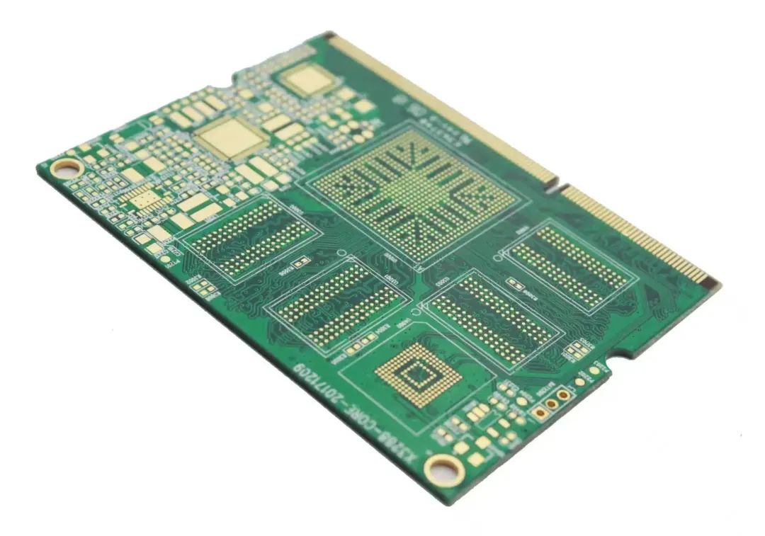
1. According to circuit layers, it can be classified into single-sided boards, double-sided boards, multi-layer boards, and HDI (High-Density Interconnect boards).
2. According to substrate types, there are paper-based PCBs, glass cloth-based PCBs, synthetic fiber PCBs, organic film substrate PCBs, ceramic substrate PCBs, and metal core PCBs.

02
Structure of PCB
PCBs mainly consist of Copper Clad Laminates (CCL), Prepreg (PP), Copper Foil, Solder Mask, Surface Treatment, and Characters.
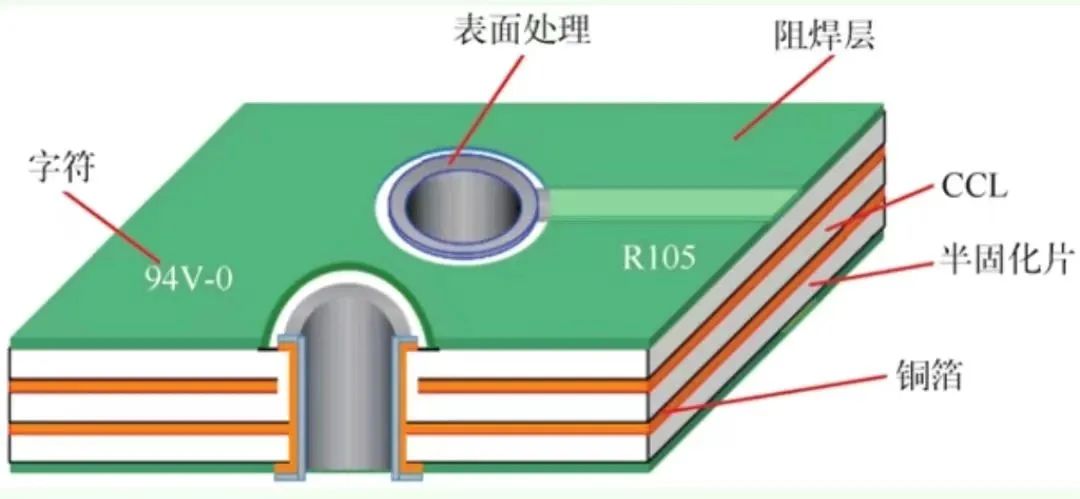
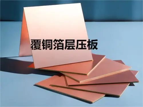
1) Copper Clad Laminates
Copper Clad Laminates (CCL), also known as copper-clad boards, are the fundamental materials for manufacturing printed circuit boards. They are composite materials made of a dielectric layer (resin, glass fiber) and high-purity conductors (copper foil). CCL provides three main functions: conduction, insulation, and support for the entire PCB. The performance, quality, and manufacturing cost of PCBs largely depend on CCL.
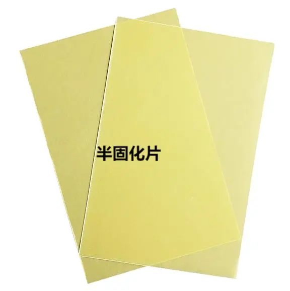
2) Prepreg
Prepreg, also known as PP, is one of the main materials in multilayer board production, primarily composed of resin and reinforcement materials. Reinforcement materials include glass fiber cloth, paper-based, and composite types. Most of the prepreg used in multilayer PCBs employs glass cloth as a reinforcement material.
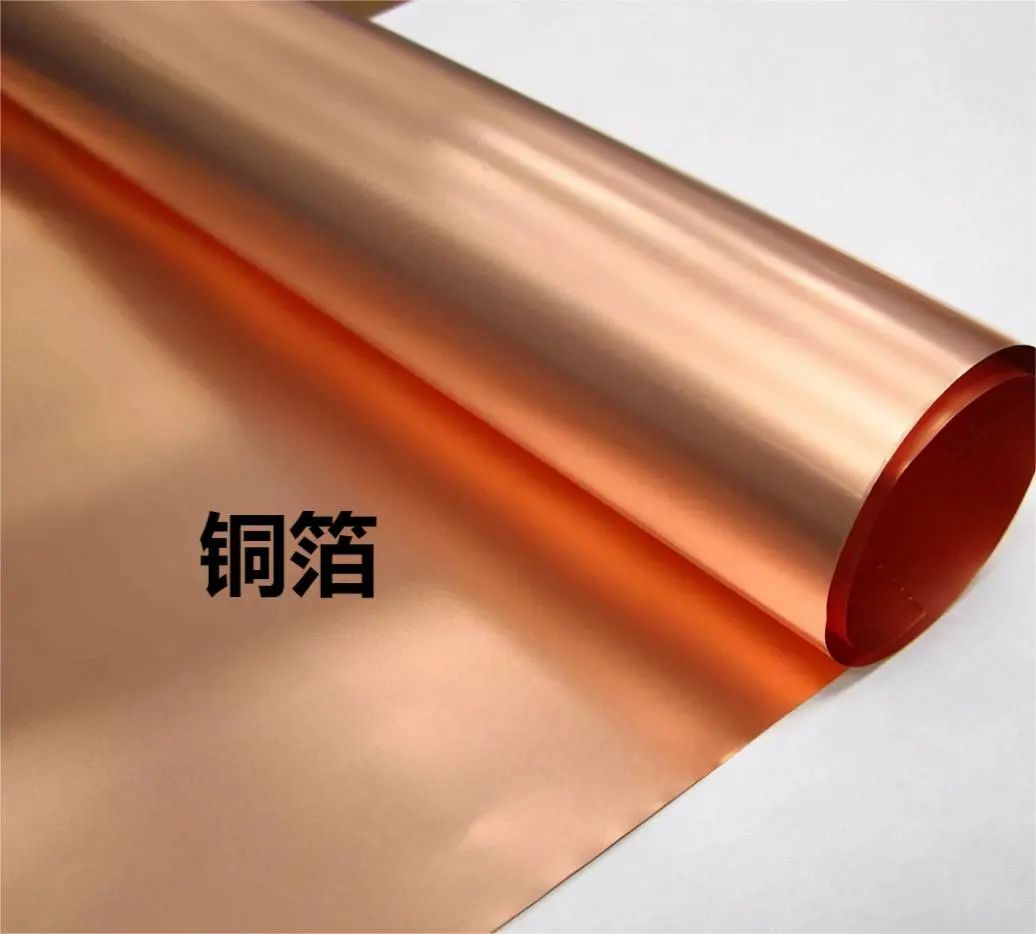
3) Copper Foil
Copper foil is a thin, continuous layer of metal deposited on the substrate layer of the circuit board. It serves as the conductor for PCBs and can be easily bonded to the insulation layer, forming circuit patterns after etching.
Common industrial copper foils can be categorized into rolled copper foil (RA copper foil) and electrolytic copper foil (ED copper foil).
Rolled copper foil has better ductility and is used in early flexible board processes.
Electrolytic copper foil has the advantage of lower manufacturing costs compared to rolled copper foil.
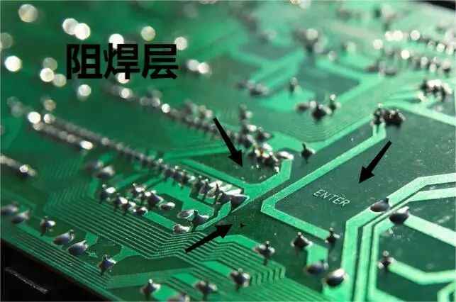
4) Solder Mask
The solder mask refers to the areas of the printed circuit board that have solder mask ink.
Solder mask ink is usually green, with some using red, black, and blue. In the PCB industry, solder mask ink is often referred to as green oil. It serves as a permanent protective layer for the printed circuit board, providing moisture, corrosion, mold, and mechanical abrasion protection, while also preventing components from being soldered in the wrong places.
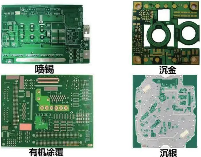
5) Surface Treatment
Since bare copper is easily oxidized and contaminated when exposed to air, a protective film is applied to the surface of bare copper. Common PCB surface treatment processes include leaded tin spraying, lead-free tin spraying, organic coating, immersion gold, immersion silver, immersion tin, and gold finger plating. With the continuous improvement of environmental regulations, leaded tin spraying has gradually been phased out.
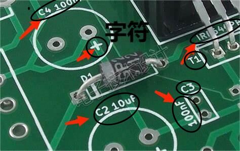
6) Characters
Characters refer to the text layer, which can be absent on the topmost layer of the PCB. Typically used for annotations, markings, and text codes are printed on the top and bottom surfaces of the printed board for installation and maintenance convenience, such as component designators, nominal values, component outlines, manufacturer logos, and production dates. Characters are usually printed using screen printing methods.

03
Applications of PCB
Almost every electronic device, from small headphones, batteries, and calculators to large computers, communication devices, airplanes, and satellites, requires PCBs for electrical interconnections between integrated circuits and other electronic components.
By adopting printed circuit boards, electronic devices avoid the errors associated with manual wiring due to the consistency of similar printed circuit boards.
Printed circuit boards provide mechanical support for fixing and assembling various electronic components such as integrated circuits, completing wiring and electrical connections or electrical insulation between them, providing the required electrical characteristics, and offering solder mask patterns for automated soldering, along with identification characters and graphics for component insertion, inspection, and maintenance.
Scan to Follow Us
/

/
WeChat ID | Biomedical Engineering Laboratory
Contributor: Huang Shuni
Final Review: Tu Peiqi