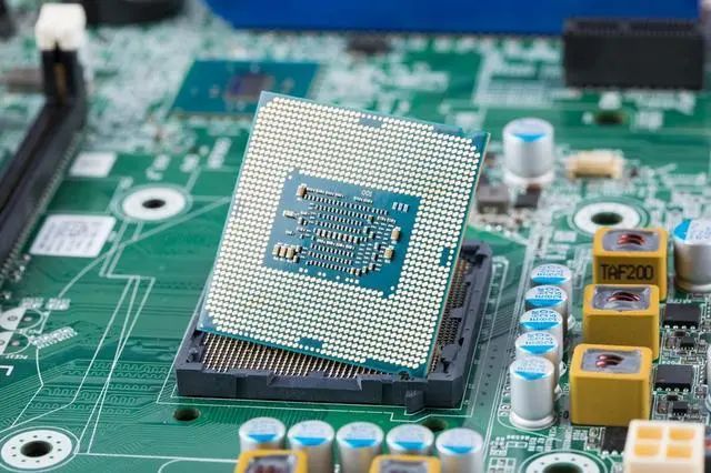
With the continuous advancement of technology, the quality control of internal PCB circuit boards has become increasingly strict, leading to a more urgent development and upgrading of PCB surface treatment technologies. This article introduces the commonly used PCB surface treatment technologies in the market today.
What Is Surface Treatment?
PCB surface treatment technology refers to the process of artificially forming a layer on the PCB components and electrical connection points that has different mechanical, physical, and chemical properties from the substrate. The purpose is to ensure good solderability and electrical performance of the PCB. Since copper tends to exist in the form of oxides in the air, which severely affects the solderability and electrical performance of the PCB, surface treatment is necessary.

Common Surface Treatment Methods
Organic Solderability Preservative (OSP)
OSP is a process for treating the surface of copper foil on printed circuit boards (PCBs) that complies with RoHS directives. OSP stands for Organic Solderability Preservatives, which translates to 有机保焊膜 in Chinese, also known as copper protector or Preflux in English. Simply put, OSP is a chemical method of growing a layer of organic film on a clean bare copper surface.
This layer of film has anti-oxidation, thermal shock resistance, and moisture resistance properties, used to protect the copper surface from further rusting (oxidation or sulfuration) in normal environments; however, during subsequent high-temperature soldering, this protective film must be easily removed by the flux quickly, allowing the exposed clean copper surface to bond immediately with the molten solder to form a strong solder joint.
Hot Air Leveling
Hot air leveling, also known as hot air solder leveling (commonly referred to as tin spraying), is a process where molten tin (lead) solder is coated on the PCB surface and leveled using heated compressed air, forming a coating layer that is resistant to copper oxidation and provides good solderability. During hot air leveling, a copper-tin intermetallic compound is formed at the junction of the solder and copper. The PCB must be submerged in the molten solder during hot air leveling; the air knife levels the liquid solder before it solidifies, minimizing the meniscus shape of the solder on the copper surface and preventing solder bridging.
Gold Plating
Gold plating involves wrapping a thick layer of electrically conductive nickel-gold alloy on the copper surface, which can protect the PCB for a long time; additionally, it has environmental resistance that other surface treatment processes do not possess. Furthermore, gold plating can prevent the dissolution of copper, which is beneficial for lead-free assembly.
The advantages include resistance to oxidation, long-term storage, and a flat surface, making it suitable for soldering fine-pitch leads and smaller components. It is the preferred choice for key PCB boards (such as mobile phone boards). It can be repeatedly subjected to reflow soldering without significantly reducing its solderability. It can also serve as a substrate for COB (Chip On Board) wire bonding.
However, the disadvantages include high costs and lower soldering strength due to the use of non-electroplated nickel processes, which can easily lead to black pad issues. The nickel layer may oxidize over time, lacking long-term reliability.
Silver Plating
Silver plating is a process that lies between OSP and chemical nickel/gold plating, being simpler and faster. It can still provide good electrical performance and maintain good solderability when exposed to hot, humid, and polluted environments, but it will lose its luster. Since there is no nickel layer beneath the silver layer, silver plating does not possess the good physical strength of chemical nickel/gold plating.
Tin Plating
The PCB tin plating process is a green and environmentally friendly new process designed specifically to facilitate SMT and chip packaging, where a tin metal coating is deposited on the copper surface via chemical methods, replacing the Pb-Sn alloy coating process, and is widely used in electronic products (such as circuit boards, electronic devices) and hardware, decorations, etc.
Nickel-Gold
(1) Chemical Nickel-Gold
A thick layer of electrically conductive nickel-gold alloy is wrapped around the copper surface, which can protect the PCB for a long time. Unlike OSP, which only serves as an anti-rust barrier, it can achieve good electrical performance during long-term use of the PCB. Additionally, it has environmental resistance that other surface treatment processes do not possess;
(2) Electroplated Nickel-Gold
In this process, a layer of nickel is electroplated onto the PCB surface conductors, followed by a layer of gold. The nickel plating mainly prevents diffusion between gold and copper. Currently, there are two types of electroplated nickel-gold: soft gold and hard gold. Soft gold is mainly used for bonding gold wires during chip packaging; hard gold is mainly used in non-soldering electrical interconnections.
Tin Spraying
(1) Leaded Tin Spraying
Leaded tin spraying refers to the process of mixing tin in a certain proportion, where lead increases the activity of the tin wire during the soldering process. Leaded tin wire is relatively easier to use compared to lead-free tin wire, but lead is toxic, and the lead in leaded tin is harmful to the human body; the eutectic temperature of leaded tin is lower than that of lead-free tin. The specific values depend on the composition of the lead-free alloy, for example, the eutectic temperature of SNAGCU is 217 degrees, and the soldering temperature is the eutectic temperature plus 30-50 degrees. It depends on the actual adjustment. The eutectic temperature of leaded tin is 183 degrees. Mechanical strength, brightness, etc., leaded tin are better than lead-free. Therefore, leaded tin is not environmentally friendly, which contradicts the global advocacy for environmental protection. Hence, lead-free tin spraying was born.
(2) Lead-Free Tin Spraying
Lead-free tin is an environmentally friendly process that poses very little harm to the human body and is currently advocated as a process where the lead content does not exceed 0.5. Lead-free tin has a higher melting point, making solder joints much more solid. In essence, leaded tin spraying and lead-free tin spraying are the same process; only the purity of lead differs. Lead-free tin is more environmentally friendly and safer for the human body and the environment, representing a future trend that is recommended for use.
PCB Mixed Surface Treatment Technology
This involves selecting two or more surface treatment methods for surface treatment, with common combinations including: nickel-gold + anti-oxidation, electroplated nickel-gold + nickel-gold, electroplated nickel-gold + hot air leveling, nickel-gold + hot air leveling, lead-free tin spraying + gold fingers.
Product Recommendations
For the challenges of process control, product quality inspection, and other aspects of PCB surface treatment, Langsheng Science offers efficient XRF analysis solutions, including a range of products: handheld, portable, and desktop RF instruments, capable of fast, efficient, non-destructive, and accurate analysis of the thickness and composition of PCB surface treatments to meet your various analytical purposes and needs.
Source: Internet
