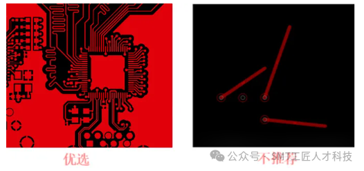
When designing PCBs, it is evident that the routing process is indispensable. The rationality of the routing not only determines the aesthetics of the PCB and its production costs but also reflects the performance of the circuit and its heat dissipation capabilities, as well as whether the performance of the components can be optimized.
This article provides a comprehensive summary of PCB routing methods.
1. The length of the trace should include the length of vias and pad soldering.
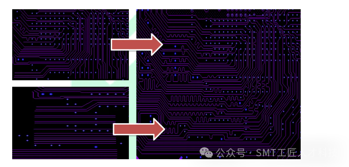
2. The preferred routing angle is 135 degrees; routing at any other angle may lead to manufacturing issues.
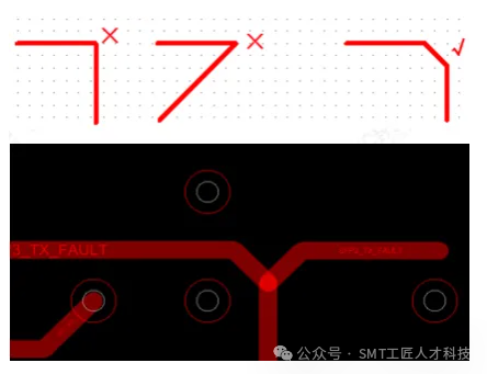
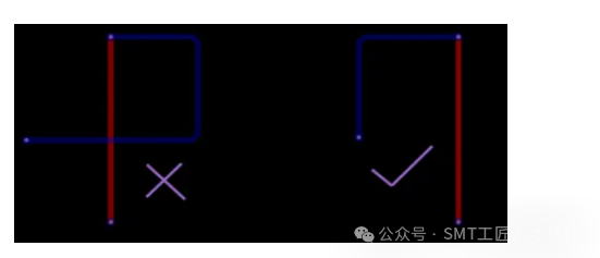
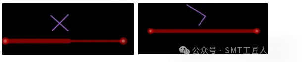
3. Avoid routing with right angles or acute angles, as this can cause changes in trace width and impedance at the corners, leading to signal reflections, as shown in the figure below.
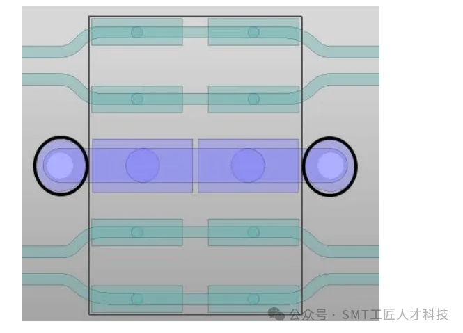
 4. Routing should exit from the long side of the pad, avoiding exits from the wide side or corners of the pad. The corner of the routing should be at least 6 mil away from the pad, as shown in the figure below.
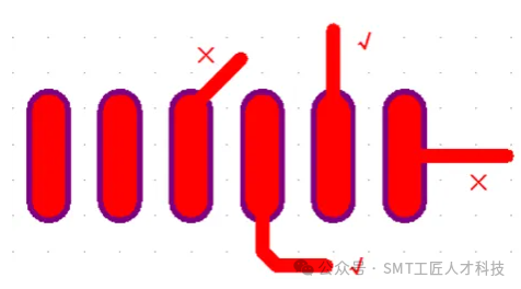
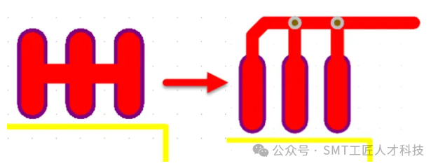
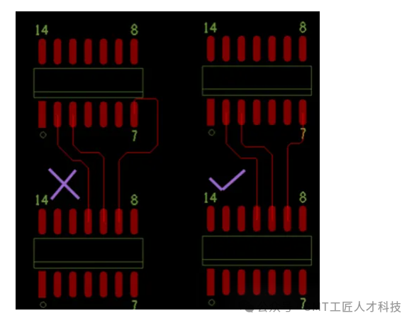
5. As shown in the figure below, adjacent pads that are part of the same network should not be directly connected. They should first connect out of the pad before making the connection, as direct connections can easily lead to solder bridging during manual soldering.
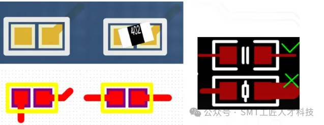
6. For small chip components, pay attention to the symmetry of the routing, keeping the trace widths of both ends consistent. For example, if one pin has copper poured, the other pin should also have copper poured to minimize component drift and rotation after placement, as shown in the figure below.
7. For signals that require ground shielding, ensure the integrity of the ground shield. It is advisable to place GND vias along the ground shield line, with a spacing of no more than 50-150 mils between two GND vias, as shown in the figure below.
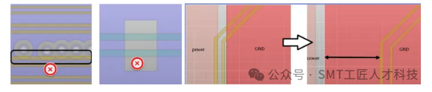
8. Traces should have a complete and continuous reference plane to avoid high-speed signals crossing regions. It is recommended that high-speed signals maintain a distance of at least 40 mils from the edge of the reference plane, as shown in the figure below.
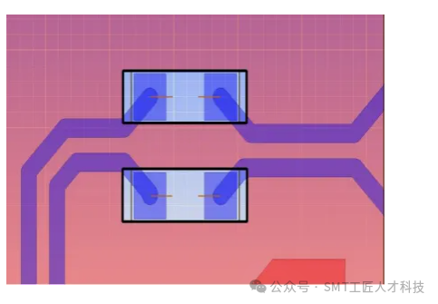
9. Due to the solder pads of surface mount devices causing impedance reduction, it is recommended to excavate a layer of reference plane directly beneath the surface mount pads to minimize the impact of impedance discontinuities. Common surface mount devices include capacitors, ESD protection, common mode choke inductors, connectors, etc., as shown in the figure below.
10. As shown in the figure below, the loop area formed by the signal line and its return path should be kept as small as possible. A smaller loop area results in lower radiation and reduced susceptibility to external interference.
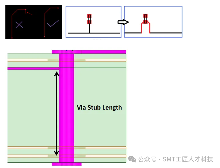
11. As shown in the figure (above), routing should not have stubs. Minimize the length of stubs, ideally keeping them at zero. Also, avoid the stub effect of vias, especially when the stub length exceeds 12 mils. It is recommended to simulate the impact of via stubs on signal integrity, as shown in the figure (below).
12. Try to avoid routing that forms self-loops across different layers. This issue is common in multilayer board designs and can cause radiated interference, as shown in the figure below.
13. It is recommended not to place test points on high-speed signals.
14. For signals that may cause interference or are sensitive (such as RF signals), shielding should be planned. The width of the shield is typically 40 mils (generally kept above 30 mils, which can be confirmed with the customer’s manufacturer), and as many GND vias as possible should be placed on the shield to enhance its soldering effectiveness.
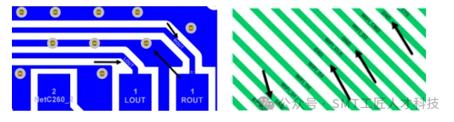
15. The trace width for the same network should remain consistent. Variations in trace width can cause uneven characteristic impedance, leading to reflections at higher transmission speeds. Under certain conditions, such as with connector lead wires or BGA package lead wires, if the spacing is too small, it may be unavoidable to have variations in trace width. Efforts should be made to minimize the effective length of inconsistent sections, as shown in the figure below.
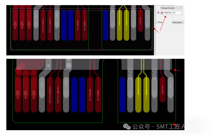
16. The trace width exiting from IC pins should be less than or equal to the pad width. The trace width cannot exceed the pad width. For some signals that require wider trace widths due to current-carrying requirements, the routing can initially match the pin width, and then increase the width by 6-10 mils after exiting the pad, as shown in the figure below.
17. Routing must connect to the center of pads and vias.
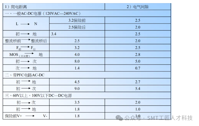
18. For high-voltage signals, ensure the creepage distance, with specific parameters shown in the figure below.
19. For designs that include multiple DDR or other memory chips, confirm the routing topology with the customer and check for any reference documentation.
20. The gold finger area needs to be treated with a full window. In multilayer board designs, all copper layers below the gold finger should be excavated, with the excavation distance from the board frame generally being more than 3 mm.
21. Routing should be planned in advance for the channel situation at bottleneck locations, ensuring reasonable routing capacity at the narrowest points.
22. Coupling capacitors should be placed as close to the connectors as possible.
23. Series resistors should be placed close to the transmitting device, while termination resistors should be placed near the end, such as series resistors on eMMC clock signals, which are recommended to be placed near the CPU side (within 400 mils).
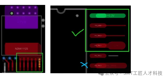
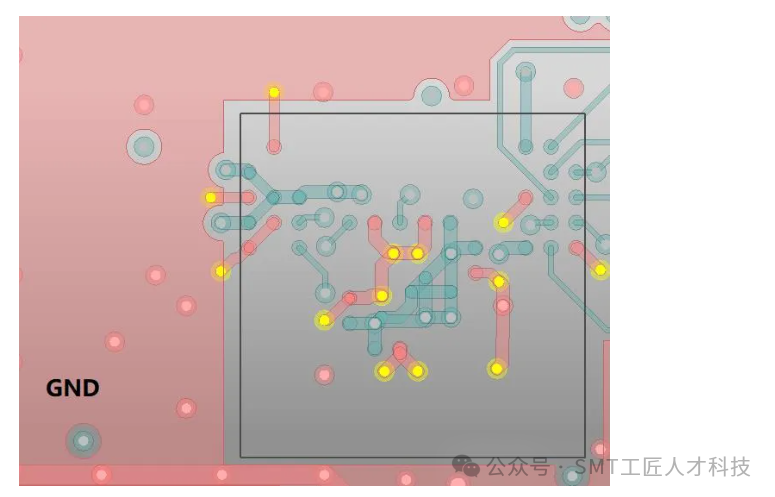
24. It is recommended to place a ground via for each ground pad of ICs (such as eMMC chips, FLASH chips, etc.) to effectively shorten the return path, as shown in the figure below.
25. It is recommended that each ground pad of ESD devices have a ground via, and the via should be as close to the pad as possible, as shown in the figure below.
26. Avoid routing near clock devices (such as crystals, oscillators, clock generators, clock distributors), switch-mode power supplies, magnetic devices, and through-hole components.
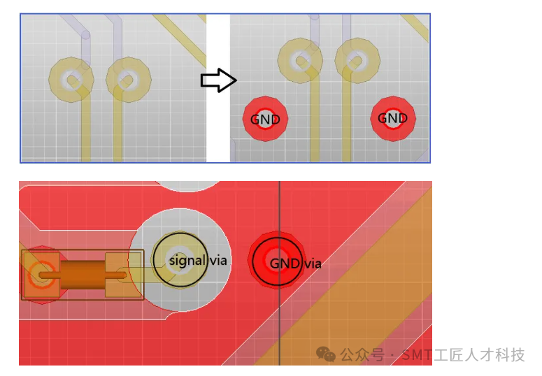
27. When changing layers, and if the reference planes before and after the layer change are ground planes, place a companion via next to the signal via to ensure continuity of the return path. For differential signals, both the signal via and return via should be symmetrically placed, as shown in the figure (above); for single-ended signals, it is recommended to place a return via next to the signal via to reduce crosstalk between vias, as shown in the figure (below).
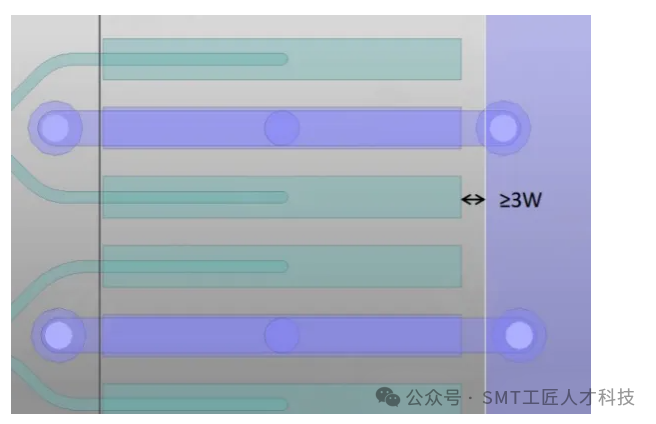
28. The distance between the ground copper of the connector and the signal pad should be at least three times the line width, as shown in the figure below.
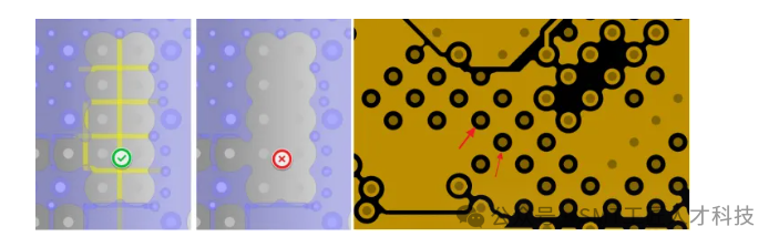
29. Use routing to connect at the plane break in the BGA area, or perform pad cutting to avoid damaging the integrity of the plane, as shown in the figure below.
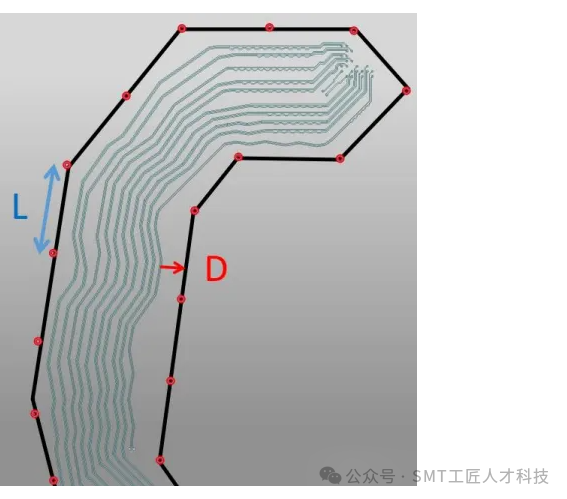
30. When ground treatment is required for PCB routing, the recommended grounding method is shown in the figure below, where L is the spacing between ground vias; D is the distance between the ground line and the signal line, recommended to be ≥4*W.
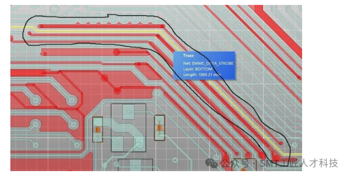
31. For some important high-speed single-ended signals, such as clock signals, reset signals, etc. (like emmc_clk, emmc_datastrobe, RGMII_CLK, etc.), it is recommended to use ground shielding. Ground vias should be placed at least every 500 mils along the ground line, as shown in the figure below.

 For those interested in learning SMT technology, please contact me!