Leakage power consumption has increased with each generation of CMOS technology. This leakage power not only poses a serious challenge for battery-powered or portable products but is also becoming an issue that wired devices such as servers, routers, and set-top boxes must address.
To reduce the total leakage power consumption of chips, it is best to implement mechanisms to turn off unused modules. This technique is known as power gating.
This chapter provides an overview of power gating, previously described from the RTL design perspective. The following sections will continue to describe how to implement power gating at the RTL level, the power gating strategies used on SALT chips, and the architectural implications of power gating. We focus on how RTL designers can design power gating in a technology-independent and portable manner.
Dynamic and Leakage Power Overview
The basic strategy of power gating is to provide two power modes: low power mode and normal mode. The goal is to switch between these modes at the appropriate time and in the appropriate manner to maximize power savings while minimizing the impact on performance.
The power reduction techniques described earlier do not affect the functionality of the design and do not require changes to the RTL. They can be handled quite transparently from a design and implementation perspective; power gating is more challenging than clock gating because it affects inter-block interface communication and introduces significant time delays to safely enter and exit power gating mode.
As part of device drivers or operating system idle tasks, control software can explicitly schedule power logic to turn logic blocks off and on. Alternatively, it can be initiated in hardware by timers or system-level power management controllers. In any case, we face architectural trade-offs:
The potential savings in leakage power.
The time cost of entering and exiting power gating.
The power consumption of entering and leaving this leakage-saving mode.
The activity ratio (the ratio and frequency of sleep or active states).
First, we introduce some terms related to entering and exiting power modes:
Sleep event: the start of entering low power mode.
Wake event: the initiation of returning to active mode.
Figure 4-1 shows an example of a subsystem that reduces power consumption using clock gating.
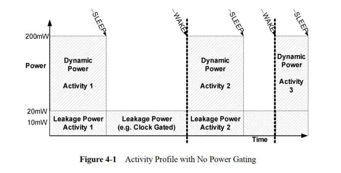
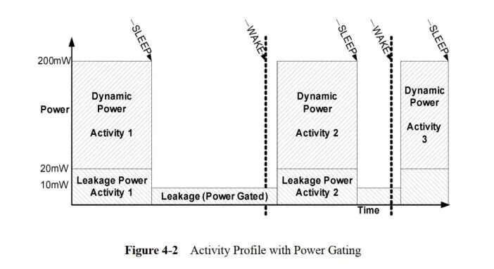
Figure 4-2 shows an example of the same subsystem implemented with basic power gating control. The response time between the wake event and the running clock can be significant and should not be overlooked at the system design level:
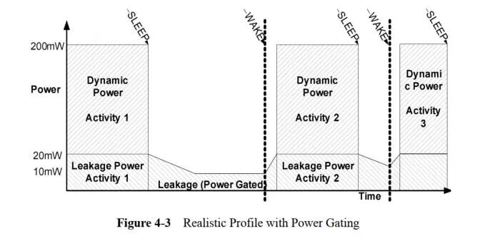
As shown in Figure 4-3, leakage power savings are not instant reductions; it takes time to reach the target level. Therefore, the achievable power savings are somewhat affected:
Impact of Clock Gating on Different Subsystems
The CPU’s cache subsystem can often remain in sleep or inactive states for extended periods, making power control very attractive. However, there are some trade-offs that must be considered:
Power gating provides excellent leakage power reduction for the entire CPU, but it has significant system-level design implications for interrupt wake-up time response (which may even require deeper FIFOs or scheduled time slots). If the cache contents are lost every time the CPU is powered off, then the time and power cost of refilling the cache upon power-up can be substantial during all bus activities. The net power savings depend on the sleep/wake activity ratio, i.e., how much energy is saved when the power is off and how much energy is spent in the reload state.
Peripheral subsystems may manage power better than the CPU. They are controlled by a power management scheme that can be optimized by device drivers and the operating system, but there are still some trade-offs. In particular, it is necessary to quickly restore state upon waking to maximize power savings:
Device drivers may need to explicitly load/restore critical states or initiate hardware program control as part of the sleep/wake sequence, but this places a significant burden on the software. A better approach may be to allow peripherals to store critical states internally while in sleep mode, but this requires special circuitry and additional control.
Finally, consider a more complex multi-processor CPU cluster where one or more processors may be completely powered off. In this case, we assume that the processor only powers off when it has completed a task and is idle, waiting for another task to be assigned. In this scenario:
Power gating can provide excellent leakage power reduction for individual CPUs. Since the CPU has already completed its task, losing local cache contents during power gating is not an issue. The CPU is awakened, cleaned, and reset, ready to execute and cache the next task. Optimized power consumption may require adaptive shutdown algorithms that change the number of power-gated and active CPU cores based on different workloads.
In all of the above cases, power gating can provide significant leakage current reduction in the design.
