Author:RimeLink
Source: http://blog.csdn.net/jiangjunjie_2005/article/details/47700597
Introduction:
Power consumption is a significant issue for battery-powered products; once the energy is depleted, the device will “stop working.” In “Low Power Design of MCUs (Part 1) Theory,” we introduced the principles of energy saving; in “Low Power Design of MCUs (Part 2) Practice,” we measured the low power consumption values of the STM8L151C8.
This article discusses low power design for wireless communication products, starting with the measured power consumption of the MCU and RF chip I/O settings, then testing the power consumption of the RF chip in different modes, and finally using the energest module of the Contiki system to track energy consumption values in real-time, concluding with a summary of low power design and prospects for low power features in wireless networking. Let’s go!
1. Introduction to Wireless Communication Products
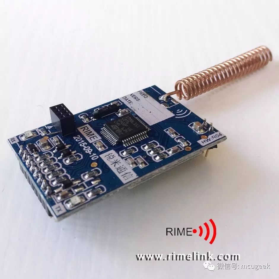
The iWL881A wireless communication module is a long-range low-power product from “Changsha Rime Communication Technology Co., Ltd. (www.rimelink.com)” (as shown below). It is embedded with the efficient and powerful IoT operating system Contiki, supporting star/tree/MESH networks, forming an “end-pipe-cloud” system with the company’s concentrator and cloud server. Typical application scenarios include: residential metering (water/electricity/gas), streetlight control, factory data collection, security alarms, etc.
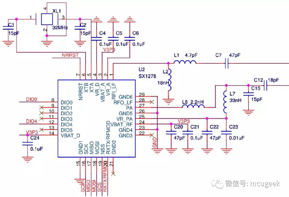
This low-power wireless communication product is primarily powered by batteries, making low power design the first “main battlefield.” The MCU selected is the ultra-low power processor STM8L151C8 from STMicroelectronics, and the RF chip (RF) is the SX1278 from Semtech, which is based on the LoRa spread spectrum communication principle, achieving nearly four times the distance compared to FSK modulation under the same conditions. For more information on the LoRa communication principle, please refer to the author’s blog post “LoRa Wireless Communication Design (Part 1) Principles.”
The MCU is connected to the RF via the SPI bus, along with some control pins. The hardware schematic of the SX1278 is shown below: RF sends notification signals to the MCU through DIO0-5 pins, while NSS/SCK/MISO/MOSI are the SPI bus, and NRRST is the MCU reset pin for the RF.
2. Static Low Power Consumption
1. MCU Pin Configuration
To achieve true low power consumption in products, the first step is to correctly configure the I/O pins, as a single I/O pin can consume milliamps. In other words, if you accidentally overlook or misconfigure an I/O pin, it will ruthlessly “devour” the results you painstakingly achieved in the MCU’s low power mode.
The MCU’s I/O pins can be roughly divided into four categories: unconnected, connected to 3.3V, IC input to MCU output, and IC output to MCU input. Next, we will conduct a series of experiments to see how to configure these four types of pins.
Experiment 1: For I/O pins connected to 3.3V, they need to be set as Output, high level. Is push-pull or open-drain more suitable? The experimental results for five I/O pins connected to 3.3V are as follows:
push-pull: 0.4 uA
open-drain: 29.3 uA
Conclusion: For I/O pins connected to 3.3V, in energy-saving mode, they should be set as Output, push-pull, high level.
Experiment 2: For 36 floating I/O pins, set them in the following six modes, with the power consumption data as follows:
Input, floating: 536 uA
Input, pull-up: 0.4 uA
Output, open-drain, low level: 0.4 uA
Output, open-drain, high-impedance level: 530 uA
Output, push-pull, low level: 0.4 uA
Output, push-pull, high level: 0.4 uA
Conclusion: Floating I/O pins can be set as: (1) Input, pull-up; (2) Output, push-pull, high (low) level.
Experiment 3: For six I/O pins connected to RF (RF as input direction), set them in the following six modes, with the power consumption as follows:
Input, floating: 489 uA
Input, pull-up: 482 uA
Output, open-drain, low level: 660 uA
Output, open-drain, high-impedance level: 494 uA
Output, push-pull, low level: 661 uA
Output, push-pull, high level: 574 uA
Conclusion: For pins where the external IC is input, in energy-saving mode, they should be set as: Input, pull-up.
Experiment 4: For nine I/O pins connected to RF (RF as output direction), set them in the following two modes, with the power consumption as follows:
Input, floating: 430 uA
Input, pull-up: 574 uA
Conclusion: For pins where the external IC is output, in energy-saving mode, they should be set as: Input, floating.
The basic principles for MCU pin configuration are summarized as follows:
|
Legend |
Characteristics |
Energy-saving Configuration Mode |
|
IC output, MCU input: Input, floating |
Input floating, no external interrupt |
|
|
IC input, MCU output: Input, pull-up |
Input pull-up, no external interrupt |
|
|
3.3V pin: Output, pull-up, high level |
Output push-pull, high level, 2MHz |
|
|
Unconnected pin: Output, pull-up, low level |
Output push-pull, low level, 2MHz |
In actual development, we can first use an Excel sheet to list the configuration requirements for the MCU pins, referencing the “subway line” colors (an invention of the British) for identification, such as:
|
No. |
I/O |
Name |
Low Power Configuration |
Function |
|
14 |
PE0 |
LORA_RXTX |
Input floating, no external interrupt |
RF output: indicates whether RF is currently receiving or transmitting |
|
15 |
PE1 |
NC |
Output push-pull, low level, 2MHz |
|
|
16 |
PE2 |
LORA_RXE |
Input pull-up, no external interrupt |
RF receiving: RXE=1, TXE=0 |
|
17 |
PE3 |
UART2_RX |
Output push-pull, low level, 2MHz |
Not used |
|
18 |
PE4 |
UART2_TX |
Output push-pull, low level, 2MHz |
|
|
19 |
PE5 |
NC |
Output push-pull, low level, 2MHz |
|
|
20 |
PD0 |
LED1 |
Output push-pull, high level, 2MHz |
External 3.3V, set push-pull high level for energy saving |
2. RF Operating Modes
For wireless communication products, the RF module (RF) is greedy in “devouring” energy. Let’s first look at the power consumption values claimed by the SX1278 official documentation:
|
Index |
1 |
2 |
3 |
4 |
|||
|
Mode |
Sleep |
Standby |
Receive |
Transmit |
|||
|
20dBm |
17dBm |
13dBm |
7dBm |
||||
|
Power Consumption |
0.2 uA |
1.6 mA |
12 mA |
120 mA |
87 mA |
29 mA |
20 mA |
In actual products, what is the overall power consumption of the MCU + RF? Let’s continue to look at the experimental data:
Experiment 5: The MCU configures all I/O pins to low power mode, sets the RF to Sleep mode via the SPI bus, turns off the SPI clock, and restores the SPI bus pins to low power mode, entering Halt.
Result: Overall power consumption = 0.6 uA.
In “Low Power Design of MCUs (Part 2) Practice,” we learned that the MCU in Halt mode consumes 0.4 uA; adding the RF in Sleep mode at 0.2 uA gives a total of 0.6 uA.
Experiment 6: The MCU configures all I/O pins to low power mode, sets the RF to Standby mode via the SPI bus, turns off the SPI clock, and restores the SPI bus pins to low power mode, entering Halt.
Result: Overall power consumption = 1.493 mA.
This 1.493 mA power consumption is due to the RF in Standby mode, as the MCU power consumption is only 0.4 uA, which can be almost ignored.
Experiment 7: The MCU configures all I/O pins to low power mode, sets the RF to Receive mode via the SPI bus (this mode can be maintained for a long time), turns off the SPI clock, and restores the SPI bus pins to low power mode, entering Halt.
Result: Overall power consumption = 15.97 mA.
When the RF is in Receive listening mode, the power consumption is nearly 16 mA, which is much greater than the MCU’s full-speed operation power consumption (about 5 mA).
Experiment 8: The MCU configures all I/O pins to low power mode, sets the RF to Transmit mode via the SPI bus, and the MCU executes the WFI (Wait for Interrupt) instruction for energy saving. After the transmission is complete, the MCU wakes up and loops to send data frames. The power consumption values for transmission power of: +20dBm on PA_BOOST and +7dBm on RFO_LF are tested:
Result: +20dBm on PA_BOOST = 123mA, +7dBm on RFO_LF = 11mA
The transmission power is astonishing, especially when the power amplifier is turned on and adjusted to maximum power of +20dBm, the current reaches 123 mA.
3. Dynamic Low Power Consumption
French SigFox and some companies in Russia often claim that wireless metering products can work for 10 years on two ordinary AA batteries. At first, it sounds like they are either boasting or have such advanced technology that it makes others feel inferior. How do they achieve this? Let’s take a look.
From the above experiments, we know that when wireless products are in Sleep mode, the power consumption is only 0.6uA, in Receive mode it is 16mA, and in TX mode it is 100mA (for ultra-long distances). The core of any wireless communication energy-saving technology is to sleep as much as possible, which will lead to extremely low average power consumption for the entire device.
Let’s look at an example. In most energy consumption meters’ wireless reading requirements: data frames are sent approximately every 15 minutes, lasting about 100ms; they can wake up within 4 seconds, meaning every 400 seconds requires a 5ms receiving listen; the rest of the time is in Sleep mode. Over a 15-minute (900 seconds) period, the energy consumption is as follows:
Sending: 100ms * 100mA = 10mA.s
Receiving: (900 / 4) * 5ms * 16mA = 18mA.s
Sleeping: 898s * 0.6uA = 0.54mA.s
Average power consumption: (10mA.s + 18mA.s + 0.54mA.s) / 900s = 0.0317mA
Assuming the total energy of two AA batteries is 3000mAH, the time until energy depletion is: 3000mAH / 0.0317mA = 94637H = 10.8 years.
From the above example, it can be seen that to extend the lifespan of wireless communication products as much as possible, the following design principles are required:
l Sleep as much as possible, and keep the power consumption in Sleep mode as low as possible;
l Reduce the listening time;
l Improve communication success rates, and avoid conflicts and retransmissions as much as possible.
Implementing the above design requires an excellent network protocol stack, especially the RDC (Radio Duty Cycle) layer algorithm to be reasonable; the foundation for the protocol stack and software operation is the operating system, confirming the rule of thumb in smart product design: “30% hardware, 70% software.”
The iWL881A uses the powerful IoT operating system Contiki and the Rime wireless communication protocol stack. The dynamic power consumption of the product uses the energest module of Contiki to track.
The Contiki system has designed the energest module for easy tracking of energy-saving designs, which can track the running time of components. Its data structure is shown in the figure below, where energest_total_time records the total running time of components, energest_current_time records the moment the component is turned on, and energest_current_mode records whether the component is currently on, with the time unit being rtimer_clock_t.
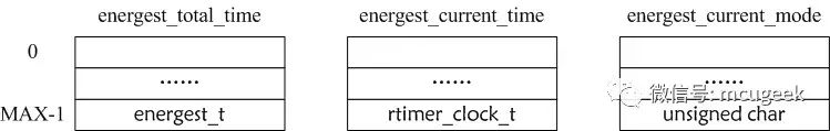
Energest data structure
When a component is turned on, call ENERGEST_ON(); when the component is turned off, call ENERGEST_OFF(). The timing logic of these two actions is shown in the figure below.
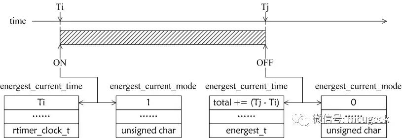
Energest timing logic
When the user needs to count the running time of components, first call the energest_flush() function, which will settle the running time of all components to the current moment; then call the energest_type_time() function to retrieve the running time of the corresponding component; finally, the energy consumption can be calculated based on the component’s power.
The iWL881A uses the energest module of Contiki to print real-time energy consumption tracking information:
CPU=5977ms, RF_TX=179ms, RF_RX=1512ms, IRQ count=30303
CPU=6023ms, RF_TX=181ms, RF_RX=1507ms, IRQ count=30304
CPU=5984ms, RF_TX=180ms, RF_RX=1497ms, IRQ count=30303
The above times are statistics over 300 seconds, indicating that: the CPU has an approximate duty cycle of 6000 / 1000 / 300 * 100% = 2%, RF transmission has an approximate duty cycle of 180 / 1000 / 300 * 100% = 0.06%, RF reception has an approximate duty cycle of 1500 / 1000 / 300 * 100% = 0.5%, and the interrupt count is about 30300 / 300 = 101 times (the test system includes a 100Hz “heartbeat” clock).
4. Networking Low Power Consumption
In the operation of wireless products in networking, there are often various communication modes such as conflict retransmission, sleep wake-up, and routing forwarding, making energy consumption tracking more challenging. Please continue to follow the “Changsha Rime Communication Technology Co., Ltd.” series of blog posts on LoRa networking.
Mouser Electronics Design Circle
The Mouser Electronics Design Circle is developed and operated by Mouser Electronics. Mouser distributes over 600 leading brands, providing a one-stop procurement platform for design engineers and procurement personnel. We welcome you to follow us for first-hand design and industry information!

MCU Development Station
Follow the latest news and related technology applications in MCU development, share insights on innovative MCU designs, and connect with MCU development experts!