State Retention and Restoration Methods
Continuing from the previous text
Low Power Design Methods – Power Gating Design (Part 1)
Low Power Design Methods – Power Gating Design (Part 2)
Given the power switch structure and isolation strategy, power gating can be applied to logic blocks. However, unless a retention strategy is employed, all state information will be lost when the module is powered off. To restore its operation upon power-up, the module must recover its state from an external source or re-establish its state from a reset condition. In either case, the required time and power consumption are significant.
In many cases, a fast and efficient way to save and restore state is through explicit retention, which can provide a quicker and more power-efficient method for the logic block to be fully operational after power is restored.
The choice of retention strategy depends on the characteristics of the subsystem. If new input data is provided, a data flow-driven digital signal processing unit may be able to start from a reset. However, peripherals or cache processors often have enough residual state that the total bus traffic required to reload this state is excessive.
There are several methods to save and restore the internal state of power-gated blocks:
One is a software method based on read/write registers.
Another is a method based on scan chains that store state externally.
Another method is using retention registers.
Using the software method, during power-down, the processor located in the always-on domain reads the registers of the power-gated block. The state information is stored in the processor’s memory block. During power-up, the processor reads the memory block and writes the state back to the power-gated block. This method has several drawbacks:
The need to use the bus significantly reduces the speed of power cycling.
Bus conflicts can make save/restore times uncertain, complicating the decision of when to turn off the power block.
Software must be written and integrated into the system software to handle power-down and power-up. This greatly reduces the reusability of the software and requires the software engineer to have a broader understanding of the hardware.
For these reasons, we will focus on the other two methods of state retention, which make power-up more transparent to the rest of the system.
State Retention Using Scan Chains
Scan chains implemented for manufacturing testing can be reused for state retention with minimal area overhead.
In this method, a set of dedicated scan chains is used for the power-gated block. During power-down, the scan registers shift as they do in scan testing, but the outputs are saved to a memory block. This memory can be on-chip or off-chip, but in either case, the memory block needs to be always powered. During power-up, the scan chain loads data from the memory block.
Note that once the state is scanned into the memory block, the entire subsystem can be powered down. There is no need for retention registers to remain powered at all times.
From an RTL design perspective, there are certainly challenges. The most basic challenge is that scan flip-flops will not be inserted and connected before synthesis—but it is necessary to encode and debug the controller at the RTL level before synthesis.
Even the number of registers and the length of the scan chains can only be known after preliminary implementation. Therefore, the control program needs to be parameterized to manage and implement the relevant counter values. It must also provide scan enable and control signals for the scan chains. These will later be linked to the netlist.
To achieve the fastest save and restore times, we want to write the retention data to memory using the full width of the data bus. This means we should make the number of scan chains equal to the width of the memory data bus. In practice, this may mean too many scan chains to be practical. However, we typically use at least 8 scan chains, and possibly multiples of 8.
If more scan chains are used, it is necessary to balance the scan chains—that is, they must all be the same length. This balance is necessary because the controller generates a single shift enable signal shared by all chains, which is also used to gate data in and out of memory. To achieve this balance, we can add extra registers on shorter chains.
Note that the memory used for retention must be large enough to accommodate the number of scanned bits. Additionally, both saving and restoring state have real-time latency costs. It grows with the size of the blocks being scanned in and out and is a function of how many scan chains are used.
There is also energy consumption in the process of moving register states out and back. If external memory is used, the IO switching power can be significant. Even with internal memory, moving data through the scan chains requires substantial dynamic power. The movement of patterns is highly dependent on state; in the worst-case scenario, every flip-flop in the block switches on every clock. This is much more switching than typical and can lead to unacceptable IR voltage drops.
Modern testing and implementation tools have had to address the fact that switching activity during scanning can be much higher than during normal operation. These tools can analyze actual IR drops and allow engineers to adjust the number of chains and clock sequences to keep IR drops at an acceptable level. However, care must be taken to avoid excessive IR drops that could corrupt data.
Despite these challenges, scan-based state retention methods can be useful in certain cases. For long-term sleep, completely powering down the entire subsystem, especially turning off external power, can significantly reduce leakage. If the state can be restored via scan chains rather than starting from a reset state upon power-up, this saving is substantial.
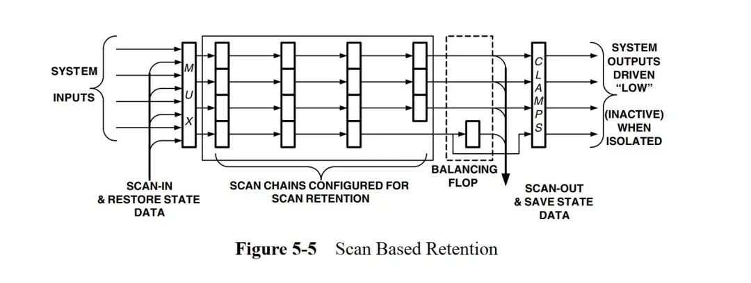
Figure 5-5 illustrates scan chain-based state saving and restoration, simplified to 4 bits for a smaller comparison. Note that one of the scan chains is shorter than the others, so an extra flip-flop is added to balance the chains. Once the scan chains are balanced, the state can be saved to the memory block (“SCAN-OUT & SAVE STATE DATA”), and then restored from the memory block (“SCAN-IN & RESTORE STATE DATA”).
Before netlist implementation (and scan insertion), functional testing and simulation at the RTL level is a challenge, but not insurmountable.
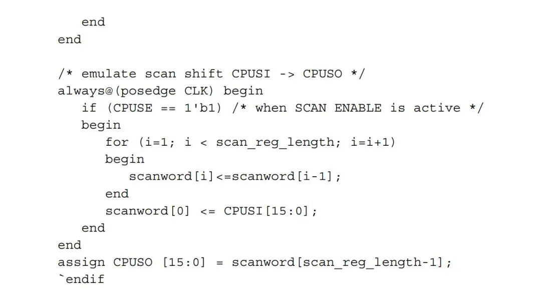
One approach is to add some conditional code in the RTL design that only compiles when simulating scan-based retention. This code simulates the behavior of shift registers and can be included in simple test sequences to verify that the controller operates correctly and that data is written to and read from memory correctly.
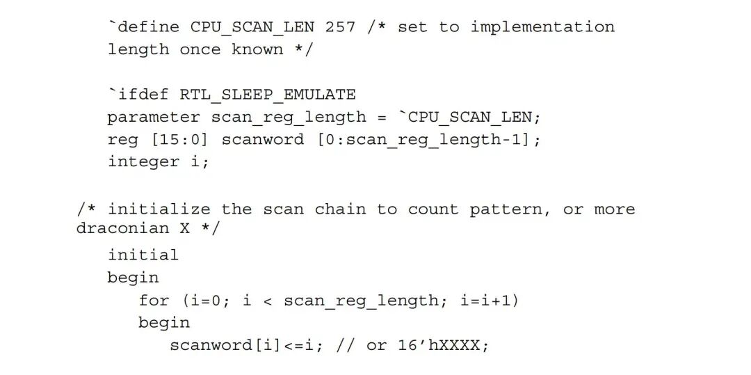
Below is an example of a virtual scan chain RTL model, which implements 16 scan chains for CPU retention. Note that virtual data is used for the scan chains.
At a later stage, gate-level netlist simulation should be performed to ensure that the implementation-specific scan chains and control signals are indeed correctly connected and that the correct length scan chains have been implemented and balanced.
