The technologies discussed in the previous chapter are mature. Engineers have been using them for some time, and design tools have supported them for many years. In this chapter, we begin to discuss more recent and proactive methods to reduce power: power gating and adaptive voltage scaling, these two techniques.
Both of these techniques differ from the traditional approach of using a single, fixed power rail for all (internal) gates in the design. (For many years, IO cells have had independent power supplies in most chips).
The most basic form of this new approach is to partition the internal logic of the chip into multiple voltage regions or power domains, each with its own voltage source. This approach is known as multi-voltage design. In modern SoC design, different blocks have different performance targets and constraints. For example, a processor may need to operate at the fastest speed allowed by semiconductor technology. In this case, a relatively high power supply voltage is required. On the other hand, a USB block may operate at a fixed, relatively low frequency, which depends more on the protocol than on the underlying technology. In this case, a lower supply voltage rail may be sufficient to meet timing requirements, and a lower voltage supply rail means its dynamic and static power consumption will be lower.
Once we overcome the conceptual barrier of using independent power supplies, we can consider more complex power strategies: for example, we can provide different voltages to the processor based on its workload. Alternatively, we can provide different voltages for RAM—maintaining a low voltage to preserve cache contents when the memory is not accessed, and a high voltage to support read and write operations. We can even consider reducing the power supply voltage to zero, known as power gating.
For the sake of discussion, we provide the following classification of multi-voltage strategies:
Static Voltage Scaling (SVS): Assigning different, fixed power supply voltages to different blocks or subsystems.
Multi-Level Voltage Scaling (MVS): An extension of static voltage scaling, where blocks or subsystems switch between two or more voltage levels for different operating modes. Only a limited number of fixed, discrete levels are supported.
Dynamic Voltage and Frequency Scaling (DVFS): An extension of MVS, which can dynamically switch between more voltage levels based on workload changes.
Adaptive Voltage Scaling (AVS): An extension of DVFS, where control loops are used to adjust the voltage.
Challenges of Multi-Voltage Domain Design
Even the simplest multi-voltage designs present some fundamental challenges for designers:
Level Shifters: Signals transmitted between blocks using different voltage supply rails often require level shifters to convert the signal from one voltage swing to another.
Description and Static Timing Analysis: If the entire chip has only one voltage source, timing analysis can be performed at a single performance point. Libraries are characterized for this point, and tools perform analysis in a straightforward manner. However, as multiple blocks operate at different voltages, and libraries may not be characterized at the exact voltages we use, timing analysis becomes more complex.
Layout Planning, Power Planning, and Grids: Multiple power domains require more careful and precise layout planning. The grid becomes more complex.
Board-Level Issues: Multi-voltage designs require additional resources, with extra regulators providing additional power.
Power-Up and Power-Down Sequences: To avoid deadlock, power design may require a specific sequence.
Voltage Scaling Interface – Level Converters
When driving signals are transmitted between voltage domains with completely different voltage rails, level converters are needed for voltage conversion. A driving signal from a 1V domain to a 5V domain may present a problem: the 1V swing may not even reach the threshold in the 5V domain. However, the internal voltage on the chip is tightly clustered around 1V. Why do we need level converters to transfer signals from a 0.9V domain to a 1.2V domain?
A fundamental reason is that a 0.9V signal driving a 1.2V gate will simultaneously turn on both NMOS and PMOS transistors, causing a short-circuit current. This issue will be discussed later in this chapter.
Additionally, the characteristics of standard cell libraries and the best operating conditions are based on a clean, fast-switching input rail. If this requirement is not met, it may lead to significant rise or fall time increases between the driving unit in one voltage domain and the receiver in another voltage domain. This, in turn, can lead to timing convergence issues and even short-circuit switching currents.
The best solution is to ensure that each domain receives the expected voltage fluctuations (as well as rise and fall times). We achieve this by providing level converters between any domains using different voltages. This approach confines any voltage fluctuation and timing characteristic issues within the boundaries of the voltage domain and does not affect the internal timing of the domain. This clean interface makes timing convergence and reuse easier.
Unidirectional Level Converters
The design of level converters can effectively provide voltage swings between different voltage rails, which is an analog circuit design issue. Due to the nature of analog circuit design, these converters are typically designed to move in one direction only—from high voltage to low voltage, or from low voltage to high voltage. In later chapters, we will provide some example designs to illustrate the differences between these two types of units.
For static voltage scaling, this unidirectional limitation of level converters is not an issue. However, for other forms of multi-voltage, the supply voltage will change during operation, which indeed poses a challenge. Designers must architect and partition the design such that the voltage domains have a clear size relationship with adjacent voltage domains, such as “always higher,” “always lower,” or “always the same.” With this constraint, appropriate level converters can be used directly. From a system perspective, designing level converters that can operate bidirectionally may be attractive, but it requires non-standard implementation components and tools.
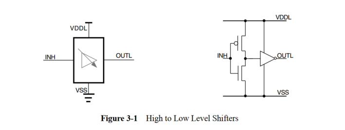
Level Converters—Voltage Conversion from High to Low
At first glance, simply outputting a signal from a buffer on a high voltage rail should not cause any issues—there are no latching or breakdown problems, and compared to standard CMOS logic high or low level switching, it would provide a “better” and faster signal edge.
However, for safe timing convergence, it is indeed necessary to include some units specifically identified as “downscaling” for this purpose. If a dedicated high-to-low level conversion unit is not provided in the process library, the entire library must be re-characterized to allow accurate static timing analysis. Each gate must have characteristics for arbitrary input voltage swings.
As shown in Figure 3-1, a high-to-low level converter can be very simple, essentially consisting of two inverters in series. The design of level converters will be described in detail in later chapters, but for now, we observe that only one voltage rail is needed, which comes from the lower or target voltage domain. As illustrated, the high-to-low level shifter only introduces a buffering delay, so its impact on timing is minimal.