This article was originally published in the Zhihu column [The Path of Digital IC Backend Engineers].
Multi-bit cells have been widely used in numerous chip designs as a means to control power consumption, and various EDA tools provide extensive and comprehensive support for them. Today, we will start with the basic structure and principles of these cells and introduce you to multi-bit cells.
As the name suggests, a multi-bit cell contains multiple logic bits within the same cell, which can also be understood as merging several identical cells into one. Taking DFF as an example, the logical relationship between single-bit and multi-bit is generally as follows (Note: the DFF shown here is a scan DFF):
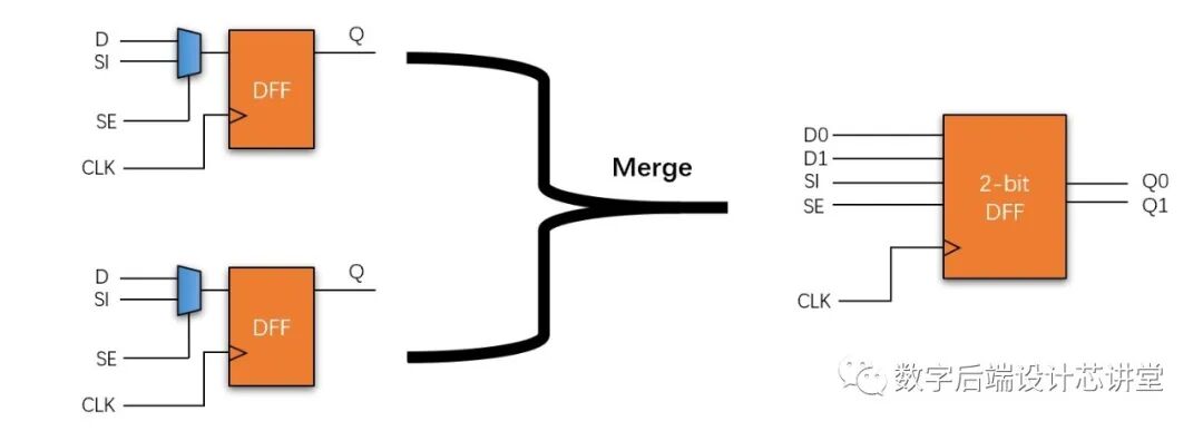
Of course, this merging is generally not a simple matter of placing two or more standard cells together, but rather a merging at the transistor level. During the layout design process at the transistor level, techniques such as optimizing transistor connections and sharing transistors are used to save area. Therefore, in many cases, multi-bit cells tend to have a smaller unit layout area compared to single-bit cells. In other words, if the area of a 1-bit DFF is  , then the area of a 2-bit DFF is generally smaller than
  , and the area of a 4-bit DFF will be significantly smaller than
  .
.
The benefits of this multi-bit structure in terms of power consumption are mainly reflected in the following aspects:
1) Reduction of clock pin capacitance, thereby lowering clock switching power.
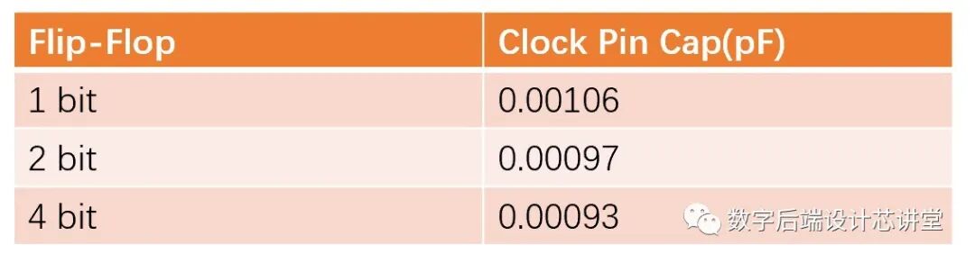
The table below lists the clock pin capacitance values for different bit DFFs of the same type. It can be seen that there is no significant difference in clock pin capacitance between single-bit and multi-bit structures. Therefore, when a design has a large number of multi-bit DFFs replacing single-bit DFFs, the overall pin capacitance value on the clock will decrease significantly. Based on our understanding of switching power, a smaller capacitance will lead to lower switching power, which will greatly contribute to reducing the overall dynamic power consumption on the clock tree.
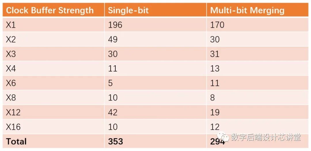
2) Reduction in the number of clock tree buffers, lowering switching and leakage power.
Since the pin capacitance of each DFF in a multi-bit DFF is significantly smaller than that of a single-bit DFF, in a multi-bit design, a single buffer can drive more bits of DFFs, thereby significantly reducing the number and area of buffers on the clock tree, further lowering power consumption on the clock tree.
3) Optimization of clock tree routing resources, effectively reducing parasitic RC in the clock tree, thereby lowering dynamic power.
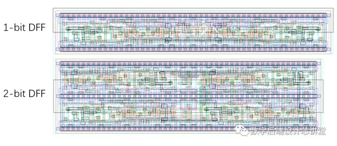
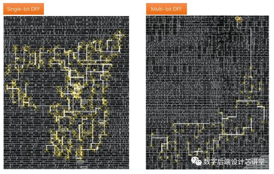
When the number of multi-bit DFFs in a design occupies a significant majority, the overall number of DFF standard cells will inevitably decrease significantly compared to a single-bit design. Moreover, in many cases, the placement of DFFs may also be more concentrated, which will save more routing resources on the clock tree, thus reducing the parasitic RC of the entire clock network. The following diagram shows a typical routing difference between a single-bit DFF and a multi-bit DFF, where it is evident that the routing on the right is significantly less. Through this method, the overall parasitic RC of the clock is reduced, thereby lowering power consumption.
Despite the numerous advantages of multi-bit cells, the best results are not always achieved in practical applications. The main reasons are as follows:
a) The conversion from single-bit to multi-bit has many conditional limitations, so in many cases, the actual ratio of multi-bit cells in the design is not high, thus failing to achieve the desired reduction in power consumption.
b) Improper placement of multi-bit cells may lead to tight routing resources, even worsening timing, which in turn may increase the power of additional combinational logic, offsetting the power reduction benefits on the clock line.
c) Considerations regarding IR/EM may intentionally place multi-bit cells further apart, thus failing to achieve the effect of reducing parasitic RC on the clock line and lowering power consumption.
This concludes our introduction to multi-bit cells. If you have any questions, feel free to leave a comment for discussion~
If you have any technical topics related to digital backend that you are interested in exploring and discussing, please scan the QR code on the left to join the digital backend communication group.
To avoid spreading advertisements, please also send verification information to answer the following question:
Besides Synopsys and Mentor, which other mainstream EDA tool vendors are there in IC design?
You are also welcome to scan the QR code on the right to follow my Zhihu:
Zhihu account : Yan Futi
Zhihu column: The Path of Digital IC Backend Design Engineers.