1.1 Overview
Over the past two decades, the design of complex chips has undergone a series of transformations. In the 1980s, language-based circuit design and synthesis emerged. In the 1990s, design reuse and IP became mainstream design practices. In recent years, low power design has begun to change the way designers handle complex SoC designs once again.
These changes are all in response to the challenges posed by the evolving semiconductor technology. The exponential growth in chip density has driven the application of language-based circuit design and synthesis, greatly enhancing the efficiency of designers. This approach has rendered Moore’s Law ineffective for about a decade, but in the era of million-gate designs, engineers found that writing new RTL for a new chip project was limited and inefficient. The result is that IP and design reuse have become the only viable methods for relatively small design teams to design large chips. Today, every SoC design incorporates a significant amount of IP to leverage the increasing density offered by submicron technology.
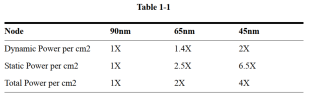
Deep submicron technology, starting from 130nm, has introduced a series of new design challenges. We can now implement tens of millions of gates on a relatively small chip, leading to power density and total power consumption reaching the limits supported by packaging, cooling, and other infrastructure. As technology has shrunk to 90nm and below, leakage current has increased dramatically, so in some 65nm designs, leakage current is nearly as significant as dynamic current.
These changes have had a significant impact on chip design. The power density of the highest performance chips has increased to such an extent that clock speeds can no longer be improved with technological advancements. Therefore, designers are now designing multiprocessor chips instead of a single ultra-high-speed processor chip.
For power supplies like batteries, this is one of the fastest-growing segments in the electronics market, but leakage caused by deep submicron processes has become a major issue in design. To address this, designers are employing advanced methods at every step of the design process, from software to architecture to implementation. These methods include power gating (turning off power when modules are not in use) and multi-threshold libraries (which can trade off leakage current for speed).
For all applications, the total power consumption of complex SoCs is a challenge. To tackle this challenge, designers are shifting from a single power supply approach (where all non-IO gates use a single power supply voltage) to a multi-power architecture, where different modules operate at different voltages depending on their respective needs. In some cases, designers use voltage scaling techniques to change the power supply voltage (and clock frequency) of critical modules based on their workload and required performance.
This book describes some techniques that designers can use to reduce power consumption in complex SoC designs. Our approach is practical rather than theoretical. Over the past few years, we have accumulated a wealth of experience while working on a series of technical demonstration chips. We believe that the techniques we describe can be used by today’s chip designers to significantly improve the chips they design.
1.2 Problem Scope
Today, some of the most powerful microprocessor chips can consume 100-150 watts. The average power density is 50-75 watts per square centimeter. Local hotspots on the chip can be several times higher than this figure.
This power density not only poses challenges for packaging and cooling; it also raises reliability issues, as the mean time to failure decreases exponentially with temperature. Additionally, circuit timing deteriorates with rising temperatures, and leakage current increases with temperature.
Historically, the power of the highest performance chips has increased with each new process technology node. However, due to power density issues, the International Technology Roadmap for Semiconductors (ITRS) predicts that the power of these chips will reach 198 watts in 2008; thereafter, power consumption will remain constant.
The total power consumption of microprocessor chips has already caused serious problems for server farms. For these server farms, infrastructure costs (power, cooling) can equal the cost of the computers themselves.
For battery-powered handheld devices, the numbers are smaller, but the issues are equally severe. According to ITRS, the battery life of these devices peaked in 2004. Since then, battery life has begun to decline as the speed of new feature additions outpaces battery upgrades.
For almost all applications, reducing SoC power consumption is crucial for improving circuit performance and ensuring the long-term viability of companies.
Until recently, power consumption was still a significant consideration in chip design. Today, for most SoC designs, the power budget is one of the most important design goals of the project. Exceeding the power budget can be fatal for the project.
As we enter the next technology node, these issues are expected to worsen. ITRS has made the following predictions:
Needless to say, many design teams are working hard to reduce power growth below these predicted numbers, as even at 90nm, many designs are at the limits of customer acceptance.
1.3 Power and Energy
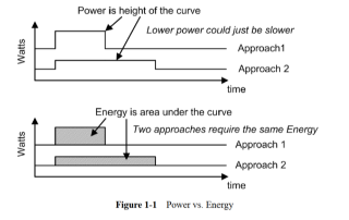
For battery-powered devices, the distinction between power and energy is crucial. As shown in Figure 1-1, power is the instantaneous power in the device. Energy is the area under the curve—energy is the integral of power over time. For example, the energy consumed by a mobile phone depends on what it is doing, whether it is in standby mode with the lid closed, or with the display on and power activated, or downloading from the internet. The height of the graph in Figure 1-1 represents power, but it is the energy—the area under the curve—that determines battery life.
1.4 Dynamic Power
The total power of SoC designs includes dynamic power and static power. Dynamic power is the power consumed when the device is active, i.e., the power consumed when signal values change. Static power refers to the power consumed when the device is powered on but there are no signal changes. In CMOS devices, static power is caused by leakage current.
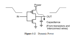
The primary source of dynamic power is switching power—the power required to charge and discharge the output capacitance on the gate. The sources of switching power are shown in Figure 1-2.
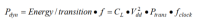
The energy required for each transition is:

Where C is the load capacitance and V is the supply voltage. We can describe dynamic power as:
Where f is the transition frequency, P is the probability of output transitions, and fclock is the frequency of the system clock. If we define:

We can also describe dynamic power using a more familiar expression:

Note that switching power is not a function of transistor size, but rather a function of switching activity and load capacitance. Therefore, it is data-dependent.
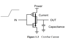
In addition to switching power, internal power also falls under dynamic power. Figure 1-3 shows the internal switching current. Internal current consists of the short-circuit current generated when both NMOS and PMOS transistors are on, as well as the current required to charge the internal capacitance of the battery.
If we add the expression for internal power into the equation, dynamic power can be described as:
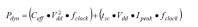
Where tsc is the duration of the short-circuit current, and Ipeak is the total internal switching current (short-circuit current plus the current required to charge the internal capacitance).
As long as the transition time of the input signal is kept short, the overall dynamic power dominated by switching power. For this reason, we often simplify the use of the dynamic power formula:

However, in some cases, short-circuit current is worth noting. Specifically, when we discuss how to handle floating outputs in power gating, we will discuss methods to prevent excessive short-circuit current.
In architecture, logic design, and circuit design, there are many techniques to reduce the power consumption of specific logic functions implemented in a given technology. These techniques focus on the voltage and frequency parameters of the modules, as well as reducing data-related switching activity.
There are various architectural and logic design techniques to optimize switching activity, effectively reducing the switching activity of the associated gates.
Due to the quadratic dependence of power consumption on voltage, reducing the supply voltage is an effective way to lower dynamic power. However, since the speed of the gate decreases with the reduction of supply voltage, this method needs to be applied cautiously. SoC designers can leverage this method in the following ways:
For blocks that do not need to run particularly fast, such as peripherals, we can supply a lower voltage than other blocks that are more speed-critical. This method is known as multi-voltage.
For processors, we can provide variable supply voltage; for tasks requiring peak performance, we can provide high supply voltage and corresponding high clock frequency. For tasks requiring lower performance, we can provide lower voltage and slower clock. This method is known as voltage scaling.
Another method to reduce dynamic power is clock gating. By reducing the frequency to zero when not needed, dynamic power is also reduced to zero. Many SoCs use some form of clock gating design.