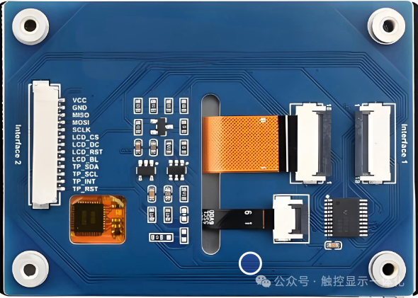
In the customer’s schematic, there are interface definitions corresponding to the motherboard. These interface definitions are provided by the customer, but we need to identify and determine the technical requirements, especially for hardware design, where it is necessary to confirm the meaning of each pin, and whether the corresponding voltage and current are compatible with our products; otherwise, changes and confirmations are required.
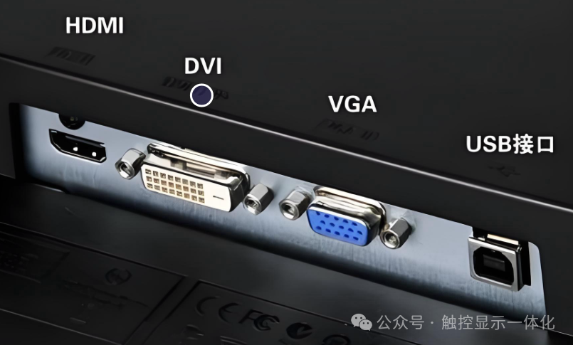
The commonly used types of touch module interfaces are shown in the table below:
| No. | Touch Module Interface Type | Applicable Conditions | Description |
| 1 | IIC | Requires pull-up resistors, medium speed, fewer pins, low cost, bottleneck in reporting rate, transmission distance short, not recommended to exceed 30cm | Conventional low-speed interface |
| 2 | SPI | Requires chip select signal, many pins, transmission distance not recommended to exceed 10cm, speed much higher than IIC, supports ultra-high reporting rate | High reporting rate interface |
| 3 | USB | Plug and play, higher cost, strong universality, supports high reporting rate, integrated power supply, generally uses IIC to USB module | Plug and play interface |
| 4 | UART | Slowest speed, low reporting rate, noticeable delay, data format needs to be customized, requires conversion IC, can transmit over long distances via RS232 interface | Long-distance interface |
Details of the touch module communication interfaces are as follows:
①IIC Interface:
| No. | Touch IIC Interface Definition | Touch IIC Interface Function |
| 1 | TP_IIC_SDA_Voltage | IIC transmission data pin, requires pull-up |
| 2 | TP_IIC_SCL_Voltage | IIC synchronous clock pin, requires pull-up |
②SPI Interface:
| No. | Touch SPI Interface Definition | Touch SPI Interface Function |
| 1 | TP_SPI_SCLK_Voltage | SPI synchronous clock pin |
| 2 | TP_SPI_MOSI_Voltage | SPI master out slave in pin |
| 3 | TP_SPI_MISO_Voltage | SPI master in slave out pin |
| 4 | TP_SPI_SS_Voltage | SPI chip select pin |
③USB Interface (Standard Interface):
| No. | Touch USB Interface Definition | Touch USB Interface Function |
| 1 | 5V | 5V power supply, USB2.0 is 500mA, USB3.0 is 1A, requires TVS tube to avoid ESD |
| 2 | D+ | USB differential data interface |
| 3 | D- | USB differential data interface |
| 4 | GND | Power ground |
④UART Interface (Requires MAX202 TTL to RS232 IC for conversion to RS232 interface):
| No. | Touch UART Interface Definition | Touch UART Interface Function |
| 1 | RS232_TX | RS232 interface transmit pin, needs to be connected to the receive pin of the main control’s RS232 interface |
| 2 | RS232_RX | RS232 interface receive pin, needs to be connected to the transmit pin of the main control’s RS232 interface |
Touch module non-communication interfaces also have the following pins::
| No. | Touch Non-communication Interface Definition | Touch Non-communication Interface Function |
| 1 | TP_VCC_Voltage | Except for the USB communication interface, all need to add a VCC power interface, and VCC must comply with the touch IC specification, and a TVS tube must be connected to avoid ESD |
| 2 | GND | Except for the USB communication interface, all need to add a power ground |
| 3 | TP_RST_Voltage | Touch IC reset pin, need to confirm whether the touch IC has a power-on reset function; otherwise, a power-on reset circuit needs to be added or connected to the same voltage main control IO control |
| 4 | TP_INT_Voltage | Touch IC sends data interrupt signal pin, often used for falling edge interrupt trigger |
| 5 | TP_IOVCC_Voltage | Used to confirm that the IO voltage of the touch IC pins such as RST/IIC/SPI/INT needs to be the same as the main control IO pin voltage, it is preferable to use the internal IOVCC voltage of the touch IC to avoid abnormal timing of the whole machine’s IOVCC leading to damage to the touch IC IO. If the customer requires compatibility with multiple motherboard IO voltages, the IOVCC pin of the touch IC needs to be connected to the IOVCC pin provided by the motherboard, but it should be reminded to the customer that the IOVCC must be powered on first. |
In order to adapt to the continuous improvement of display module resolution and refresh rate, the interface types of display modules are also continuously upgraded and changed. The commonly used display module interface types are shown in the table below:
| No. | Display Module Interface Type | Applicable Conditions | Description |
| 1 | MCU (8080/6800) | Driver IC has built-in video memory RAM, transmits image data to video memory, low resolution, low refresh rate | Parallel interface, below 320*320 |
| 2 | RGB (RGB565/RGB666/RGB888) | Relies on the motherboard memory to provide video memory, directly transmits pixel data through synchronization signals | Parallel interface, below 800*800 |
| 3 | SPI+RGB | SPI transmits driver IC initialization data, RGB transmits image data | Serial parallel, below 1080*1920 |
| 4 | IIC | Driver IC has built-in video memory RAM, transmits image data to video memory, low resolution, low refresh rate | Serial interface, below 128*128 |
| 5 | UART | Used for serial screens, only transmits text data of the serial screen, UI images are integrated into the serial screen | External interface, requires conversion IC |
| 6 | SPI (SPI three-wire/SPI four-wire/SPI 2data) | Low transmission speed, SPI 2 data lane is the fastest in SPI, ST7796PI supports | Serial interface, below 320*480 |
| 7 | QSPI | Transmission speed is faster than SPI interface with 4 data lanes, JD9161C supports | Serial interface, below 480*480 |
| 8 | LVDS | Differential transmission, can transmit over 10 meters, strong anti-interference ability | Serial interface, below 2K |
| 9 | MIPI | High-speed differential transmission, transmission distance not recommended to exceed 20cm, supports high resolution | Serial interface, below 2K |
| 10 | EDP | Multi-data high-speed transmission with low electromagnetic interference, gradually replacing low-voltage differential LVDS interfaces | External interface, below 4K |
| 11 | HDMI | High-definition multimedia interface, can transmit audio and video simultaneously, supports HDCP copyright protection | External interface, requires conversion IC, 8K |
| 12 | USB | A single USB3.0 line completes power supply and video transmission, requires low-power display module | External interface requires conversion, 1080P |
Details of the display module communication interfaces are as follows:
①MCU Interface (Commonly used 8080 MCU 8-bit):
| No. | Display MCU 8-bit Interface Definition | Display MCU 8-bit Interface Function |
| 1 | D0 | MCU 8-bit parallel transmission line |
| 2 | D1 | MCU 8-bit parallel transmission line |
| 3 | D2 | MCU 8-bit parallel transmission line |
| 4 | D3 | MCU 8-bit parallel transmission line |
| 5 | D4 | MCU 8-bit parallel transmission line |
| 6 | D5 | MCU 8-bit parallel transmission line |
| 7 | D6 | MCU 8-bit parallel transmission line |
| 8 | D7 | MCU 8-bit parallel transmission line |
| 9 | CS | Chip select signal, selects the display module |
| 10 | DC | Data/command selection signal |
| 11 | WR | Write enable signal, writes data to the display module |
| 12 | RD | Read enable signal, reads data from the display module |
②RGB Interface (Commonly used RGB888):
| No. | Display RGB888 Interface Definition | Display RGB888 Interface Function |
| 1 | B0-B7 | Blue data pin |
| 2 | G0-G7 | Green data pin |
| 3 | R0-R7 | Red data pin |
| 4 | HSYNC | Line synchronization |
| 5 | VSYNC | Column synchronization |
| 6 | DCLK | Pixel clock |
| 7 | DE | Data enable |
| 8 | STBYB | Status bit, since there is no initialization, this bit is equivalent to giving the screen 1129 or 2810 |
③SPI+RGB Interface (SPI three-wire sends initialization code + RGB565 sends data):
| No. | Display SPI three-wire + RGB565 Interface Definition | Display SPI three-wire + RGB565 Interface Function |
| 1 | B0-B4 | RGB blue data pin |
| 2 | G0-G5 | RGB green data pin |
| 3 | R0-R4 | RGB red data pin |
| 4 | HSYNC | RGB line synchronization |
| 5 | VSYNC | RGB column synchronization |
| 6 | DCLK | RGB pixel clock |
| 7 | DE | RGB data enable |
| 8 | LCM_SPI_CS | SPI chip select signal |
| 9 | LCM_SPI_SCK | SPI clock signal |
| 10 | LCM_SPI_SDA | SPI data pin |
④IIC Interface:
| No. | Display IIC Interface Definition | Display IIC Interface Function, requires IIC address |
| 1 | LCM_IIC_SDA_Voltage | Data pin |
| 2 | LCM_IIC_SCL_Voltage | Clock pin |
⑤UART Interface (mostly TTL, if RS232 then conversion is needed):
| No. | Display UART Interface Definition | Display UART Interface Function |
| 1 | TX | Transmit pin, needs to be connected to the main control’s receive pin |
| 2 | RX | Receive pin, needs to be connected to the main control’s transmit pin |
⑥SPI Interface:
| No. | Display SPI three-wire Interface Definition | Display SPI three-wire Interface Function |
| 1 | LCM_SPI_CS | SPI chip select signal |
| 2 | LCM_SPI_SCK | SPI clock signal |
| 3 | LCM_SPI_SDA | SPI data pin, data input to the display driver IC |
| No. | Display SPI four-wire Interface Definition | Display SPI four-wire Interface Function |
| 1 | LCM_SPI_CS | SPI chip select signal |
| 2 | LCM_SPI_SCK | SPI clock signal |
| 3 | LCM_SPI_SDA | SPI data pin, data input to the display driver IC |
| 4 | LCM_SPI_DC | SPI data/command selection pin |
| No. | Display SPI 2DATA Interface Definition | Display SPI 2DATA Interface Function |
| 1 | LCM_SPI_CS | SPI chip select signal |
| 2 | LCM_SPI_SCK | SPI clock signal |
| 3 | LCM_SPI_SDA1 | SPI data pin 1, data input to the display driver IC |
| 4 | LCM_SPI_SDA2 | SPI data pin 2, data input to the display driver IC |
Among them, the SPI 2DATA speed is twice that of SPI three-wire and four-wire, which can support higher refresh rates suitable for Bluetooth motherboard solutions, the display driver IC ST7796PI supports; among all the above SPI interfaces, there is actually one SDO pin used to read data from the driver IC, if there is no need to read data from the driver IC, this pin can be left floating.
⑦QSPI Interface:
| No. | Display QSPI Interface Definition | Display QSPI Interface Function, requires QSPI address |
| 1 | LCM_QSPI_CS | QSPI chip select signal |
| 2 | LCM_QSPI_SCK | QSPI clock signal |
| 3 | IO0 | QSPI data pin 1 and transmits initialization command |
| 4 | IO1 | QSPI data pin 2 |
| 5 | IO2 | QSPI data pin 3 |
| 6 | IO3 | QSPI data pin 4 |
QSPI speed is much higher than SPI and can support higher resolution and refresh rates. The display driver ICs that support QSPI include Tianyu JD9161C (480*480/800), and Xinxiangwei NV3041A-01 (480*272).
⑧LVDS Interface:
| No. | Display LVDS Interface Definition | Display LVDS Interface Function |
| 1 | RCLK+ | Clock pin differential signal |
| 2 | RCLK- | Clock pin differential signal |
| 3 | R0+ | Data pin 0 differential signal |
| 4 | R0- | Data pin 0 differential signal |
| 5 | R1+ | Data pin 1 differential signal |
| 6 | R1- | Data pin 1 differential signal |
| 7 | R2+ | Data pin 2 differential signal |
| 8 | R2- | Data pin 2 differential signal |
| 9 | R3+ | Data pin 3 differential signal |
| 10 | R3- | Data pin 3 differential signal |
⑨MIPI Interface:
| No. | Display MIPI Interface Definition | Display MIPI Interface Function |
| 1 | DCLK+ | Clock pin differential signal |
| 2 | DCLK- | Clock pin differential signal |
| 3 | D0+ | Data pin 0 differential signal |
| 4 | D0- | Data pin 0 differential signal |
| 5 | D1+ | Data pin 1 differential signal |
| 6 | D1- | Data pin 1 differential signal |
| 7 | D2+ | Data pin 2 differential signal |
| 8 | D2- | Data pin 2 differential signal |
| 9 | D3+ | Data pin 3 differential signal |
| 10 | D3- | Data pin 3 differential signal |
⑩EDP Interface:
| No. | Display EDP Interface Definition | Display EDP Interface Function |
| 1 | AUX+ | Auxiliary differential channel, used for link management, EDID reading, LCM control, etc. |
| 2 | AUX- | Auxiliary differential channel, used for link management, EDID reading, LCM control, etc. |
| 3 | L0+ | Data pin 0 differential signal, Note: For low-resolution panels (such as HD/FHD), only 1 or 2 channels may be used |
| 4 | L0- | Data pin 0 differential signal |
| 5 | L1+ | Data pin 1 differential signal |
| 6 | L1- | Data pin 1 differential signal |
| 7 | L2+ | Data pin 2 differential signal |
| 8 | L2- | Data pin 2 differential signal |
| 9 | L3+ | Data pin 3 differential signal |
| 10 | L3- | Data pin 3 differential signal |
| 11 | HPD | Hot plug detection, informs the signal source that the display module is ready |
⑪HDMI Interface (Standard Interface, requires conversion scheme):
| No. | Display HDMI Interface Definition | Display HDMI Interface Function |
| 1 | TMDS Data2+ | Red differential signal data channel 2 |
| 2 | TMDS Data2 Shield | Shielding layer for data channel 2 (ground) |
| 3 | TMDS Data2- | Red differential signal data channel 2 |
| 4 | TMDS Data1+ | Green differential signal data channel 1 |
| 5 | TMDS Data1 Shield | Shielding layer for data channel 1 (ground) |
| 6 | TMDS Data1- | Green differential signal data channel 1 |
| 7 | TMDS Data0+ | Blue differential signal data channel 0 |
| 8 | TMDS Data0 Shield | Shielding layer for data channel 0 (ground) |
| 9 | TMDS Data0- | Blue differential signal data channel 0 |
| 10 | TMDS Clock+ | Pixel clock differential signal |
| 11 | TMDS Clock Shield | Shielding layer for clock signal |
| 12 | TMDS Clock- | Pixel clock differential signal |
| 13 | CEC | Consumer Electronics Control channel, used for inter-device linkage |
| 14 | Utility | Reserved pin (function may vary in different versions, usually unused) |
| 15 | SCL | DDC clock line, used for EDID and HDCP communication |
| 16 | SDA | DDC data line, used for EDID and HDCP communication |
| 17 | Ground | Ground for DDC and CEC signals |
| 18 | 5V Power | +5V power supply (maximum 50mA), used to power the receiving chip |
| 19 | HPD | Hot plug detection, notifies the signal source that the display has been connected |
⑫USB Interface (Standard Interface, requires conversion scheme, USB3.0 used for display):
| No. | Display USB3.0 Interface Definition | Display USB3.0 Interface Function |
| 1 | VBUS | Power (+5V, 900mA) |
| 2 | D- | USB 2.0 differential data negative, can be used for touch models |
| 3 | D+ | USB 2.0 differential data positive, can be used for touch models |
| 4 | ID | Usually floating or grounded on Micro-B port (used to identify master/slave devices) |
| 5 | GND | Power ground |
| 6 | SSTX- | USB 3.0 superspeed transmit differential negative, used to read display module information |
| 7 | SSTX+ | USB 3.0 superspeed transmit differential positive, used to read display module information |
| 8 | GND_DRAIN | Signal ground/drain line |
| 9 | SSRX- | USB 3.0 superspeed receive differential negative, used for transmitting display data |
| 10 | SSRX+ | USB 3.0 superspeed receive differential positive, used for transmitting display data |
Display module non-communication interfaces also have the following pins:
| No. | Display Non-communication Interface Definition | Display Non-communication Interface Function |
| 1 | LCM_IOVCC_Voltage | Voltage for logic circuits such as IO voltage |
| 2 | VCC_Voltage | Power supply voltage |
| 3 | AVEE_Voltage | Positive power supply voltage for analog circuits, same as VSN, -5.5V~-5.8V, the larger the driving current, the better |
| 4 | AVDD_Voltage | Negative power supply voltage for analog circuits, same as VSP, 5.5V~5.8V, the larger the driving current, the better |
| 5 | VPP_Voltage | OTP programming voltage |
| 6 | VGH_Voltage | Voltage for Gate High, LCM TFT’s gate high-level positive voltage used to turn on TFT |
| 7 | VGL_Voltage | Voltage for Gate Low, LCM TFT’s gate low-level negative voltage used to turn off TFT, INCELL products need to connect a TVS tube |
| 8 | LEDK | Negative of the backlight constant current source circuit |
| 9 | LEDA | Positive of the backlight constant current source circuit |
| 10 | LCM_RST_Voltage | Reset pin of the driver IC, needs to match the voltage of IOVCC and needs to be connected in series with a 1K resistor for current limiting and filtering, otherwise, it may cause the display driver IC to overheat |
| 11 | LCM_TE | Synchronization pin, can be used to detect the frame rate of the display module, needs to be connected in series with a 1K resistor for current limiting and filtering |
| 12 | LCM_ID | Identification pin used to distinguish different modules, needs to confirm the ID voltage required by the customer |
| 13 | GND | Power ground |
| 14 | LCM_PWM | Controls the brightness of the backlight for PWM dimming and needs to be connected in series with a 1K resistor for current limiting and filtering |
| 15 |
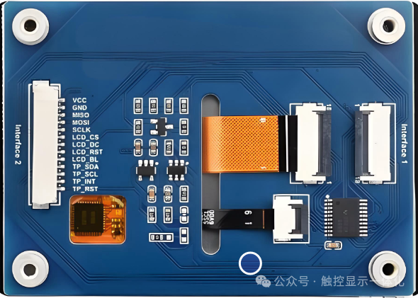
The definitions of the above touch display interfaces need to be standardized against customer drawings and internal drawings to facilitate unified identification and management, avoiding product hazards caused by incorrect voltage and current identification. If the customer drawing requires NC for the PIN, the definition of the PIN in the structural diagram needs to be deleted and cleared instead of marking it as NC in the original definition, thus avoiding misjudgment of the number of channels and other identification anomalies during electronic design.
It is worth noting that the touch module is designed to match the display module. Under the same size, the higher the resolution of the display module, the smaller the corresponding UI or icons, and the more touch channels are required, meaning the pitch needs to be smaller, with the touch area size = pitch/2.
3. Interface Speed Calculation:
The calculation formula for the size of one frame of data for the touch module = (number of touch points * 5) + 2 bytes of header. For 10 touch points, the length of one frame of data for the touch module is 10*5+2=52 bytes, with one byte being 8 bits.
If the touch reporting rate needs to be 100HZ, then the required touch interface speed is 52*8*100=41600bps≈5KB/S to meet the requirement. To increase the interface speed, the interface type can be changed, the number of touch points can be reduced, the reporting rate can be lowered, or a touch IC with a higher reporting rate can be replaced.
One pixel of the display module contains 3 sub-pixels, namely RGB red, green, and blue, corresponding to sub-pixel formats of RGB565/RGB666/RGB888. The calculation formula for the size of one frame of data for the display module = V_total x H_total x bits of RGB, for example, for a resolution of 480*800 using the data format RGB565, the minimum size of one frame is 480*800*16=6144000 bits=768000 bytes=750KB, where V_total=VS+VBP+VADR+VFP, H_total=HS+HBP+HADR+HFP. The actual calculation of the display module interface speed needs to consider these porch parameters.The porch parameters define the blank time interval between the synchronization signals (such as line synchronization and field synchronization) and the valid pixel data, which serves as a buffer area for signal switching, preventing display anomalies such as tearing or flickering.
The porch screen parameters include the following 6: The horizontal porch controls the transmission rhythm of each row of pixels, while the vertical porch controls the refresh rhythm of the entire screen frame.
- Horizontal Back Porch HBP: Refers to the time interval from the end of the line synchronization signal to the start of valid pixel data. It acts as a “backward buffer” to ensure that there is enough time for the data to stabilize after the synchronization signal switches.
- Horizontal Front Porch HFP: Refers to the time interval from the end of valid pixel data to the start of the next line synchronization signal. It acts as a “forward buffer” to prepare for the next synchronization cycle.
- Horizontal Synchronization Pulse Width HS: Refers to the duration of the line synchronization signal itself, used to mark the start or end of a line.
- Vertical Back Porch VBP: Refers to the time interval from the end of the field synchronization signal to the start of valid pixel data. Similar to the horizontal direction, it provides stabilization time after field synchronization.
- Vertical Front Porch VFP: Refers to the time interval from the end of valid pixel data to the start of the next field synchronization signal, ensuring smoothness in field switching.
- Vertical Synchronization Pulse Width VS: Refers to the duration of the field synchronization signal, used to mark the start or end of a frame image.
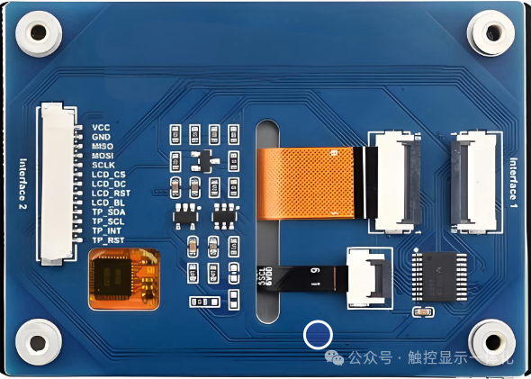
If the frame rate of the display module is 60HZ, then the transmission speed for a resolution of 480*800 using the data format RGB565, without considering the porch, would be approximately750KB*60≈44MB/S. If using 4 channels, the interface speed would need to be divided by 4. To increase the interface speed, the RGB bit depth can be changed, the frame rate can be lowered, or the porch screen parameters can be minimized.
4. Interface Conversion Solutions:
If some products do not match the customer’s required interface, the following solutions can be used for conversion:
| No. | Conversion Solution | Description |
| 1 | Requires special ICs such as domestic multi-interface types like Tianyu, Xinxiangwei, Guanhaiwei display driver ICs, which also have corresponding cost advantages, touch ICs from Yili, Xinchang, etc. | Low cost, low threshold |
| 2 | Use FPGA solutions for signal conversion, which can be designed on FPC, such as high cloud, Jingwei Qili FPGA manufacturers, requires debugging fees or minimum order quantities, and FPGA costs are relatively high, generally only used for converting non-standard interfaces of display driver ICs | Highest cost, highest threshold |
| 3 | Use dedicated conversion solutions that require dedicated PCB boards, generally converting external standard interfaces to the interfaces required by the display module or using Qinheng’s IUSB IC for IIC to USB conversion | Medium cost, medium threshold |
Major brands for dedicated display interface conversion solutions include: TI, TOSHIBA, Lontium
-
TI bridging solutions:https://www.ti.com/interface/hdmi-displayport-mipi/products.html#p1241=Bridge
Example: SN65DSI84 MIPI® DSI Bridge To FLATLINK™ LVDS Single Channel DSI to Dual-Link LVDS Bridge, single-channel 4-lane MIPI, converts to single-channel or dual-channel LVDS signals.
-
Toshiba: Full series solutions for MIPI, LVDS, DP port interconversion:https://toshiba.semicon-storage.com
-
Domestic Lontium solutions:http://www.lontiumsemi.com/product
5. Impedance matching, differential equal length, arc routing:
IIC/SPI interfaces require equal length and arc routing to avoid signal delay and interference; the routing impedance requirement for LVDS is 100 ohms based on the definition of LVDS (Low Voltage Differential Signaling) levels. The maximum amplitude of the LVDS differential signal PN is 350mV, and the internal constant current source current is 3.5mA. Therefore, the terminal matching resistance is 100 Ohm, which means the equivalent impedance between PN is 100 ohms. This is stipulated by the protocol.If it is less than 100 ohms, the terminal output level amplitude is insufficient.If it is greater than 100 ohms, the current source’s pull-out power (driving capability) is insufficient, making it susceptible to interference.
EDP/MIPI/HDMI/USB also have differential signals, requiring differential equal length and impedance matching similar to LVDS interfaces. If there are impedance anomalies, the display screen frame rate can be lowered to between 50-55 to avoid black screen issues on some displays. Synchronization can adjust the driver IC for communication interface speed and clk waveform settings to avoid communication waveform anomalies leading to black screens on some products.
Requirements for differential equal length routing: At least ensure a spacing of 3 times the line width for routing; in environments with strict timing requirements, this can be increased to 5 times the line width spacing. (2) When routing, try to increase the routing height and reduce the number of routes.