PCB (Printed Circuit Board) is the cornerstone of modern electronic devices, and its manufacturing process is a complex discipline that integrates precision machinery, fine chemicals, and microelectronics technology.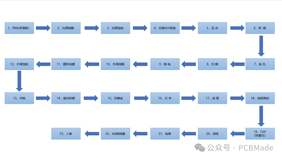
🎯 Design Output and Substrate Preparation
The PCB manufacturing process begins with the conversion of design data. The Gerber files generated by design software contain all necessary information such as layer traces and drill hole locations, serving as the benchmark for all subsequent processes.The substrate is typically made of Copper Clad Laminate (CCL), which is created by laminating copper foil onto an insulating substrate (such as FR-4 fiberglass epoxy resin). The first step in manufacturing is material cutting, where large sheets of copper-clad laminate are cut into sizes suitable for processing on the production line.
🖼️ Inner Layer Circuit Fabrication
For multilayer boards, the next step is to fabricate the inner layer circuits. The core process is graphic transfer, which aims to accurately replicate the designed circuit patterns onto the copper-clad laminate. Modern precision PCB manufacturing primarily uses the photoresist dry film method. The basic process is: a photoresist dry film is applied to the cleaned copper-clad laminate, and then the circuit pattern from a film (or directly from a laser) is transferred onto the photoresist dry film using ultraviolet light (the exposed areas undergo a polymerization reaction and harden). The unexposed parts of the dry film are then dissolved through development, leaving the copper areas that need to be preserved covered by a corrosion-resistant photoresist film. Next, inner layer etching is performed, using a chemical solution (such as acidic copper chloride) to remove the copper foil from the non-circuit areas, and finally, the film is removed, leaving a clear inner layer circuit pattern. After completion, an Automated Optical Inspection (AOI) machine compares the PCB with the original schematic to ensure there are no defects in the inner layer circuits.
🔩 Lamination and Drilling
For multilayer boards, the prepared inner core boards, prepreg (PP sheets), and copper foils need to be stacked in the design order and laminated under high temperature and pressure to form a single unit.After lamination, drilling is required, which includes component insertion holes, vias (through holes, blind holes, buried holes), etc. Drilling is a critical step in PCB manufacturing, requiring extremely high precision, typically performed by computer-controlled drilling machines or laser drilling machines, laying the foundation for subsequent inter-layer connections and component installations.
⚡ Hole Metallization and Plating
The walls of the drilled holes are insulated and require hole metallization (also known as copper plating), which involves chemically depositing a thin layer of copper (about one micron thick) on the hole walls to achieve electrical interconnection between different conductive layers. This is key for reliable interconnection in double-sided/multilayer PCBs.Subsequently, plating is performed to thicken the copper layers inside the holes and on the board surface, ensuring mechanical strength and conductivity. Sometimes, pattern plating is used to locally thicken the traces and holes before etching.
🧪 Outer Layer Fabrication and Etching
The outer layer graphic transfer is similar to the inner layer. After completing the hole metallization, an outer dry film is applied to the board, exposed, and developed, followed by pattern plating: thickening the exposed copper traces and holes (such as copper plating, followed by tin or tin-lead alloy as an anti-corrosion protective layer), and then removing the film.Next is outer layer etching, where a chemical solution is used to remove the copper foil from the non-circuit areas, leaving the copper foil of the traces protected by tin, forming the final outer layer circuit pattern. The tin layer is then removed.
🛡️ Solder Mask and Silkscreen
To prevent short circuits during soldering and protect the traces from environmental impacts, a solder mask (commonly known as “green oil”) is applied to the traces, and the areas that need to be soldered, such as pads, are exposed through exposure and development.Subsequently, silkscreen characters (such as component designators, polarity markings, version numbers, etc.) are printed on the board surface for identification during component insertion, inspection, and maintenance.
✨ Surface Treatment and Final Testing
To protect the exposed copper pads from oxidation and ensure good solderability, surface treatment is required for the bare pads. Common methods include:
- HASL (Hot Air Solder Leveling): Soldering pads are coated with tin-lead alloy and leveled with hot air, which is cost-effective but not suitable for fine-pitch components.
- ENIG (Electroless Nickel Immersion Gold): Chemically deposited nickel-gold layer, providing a flat surface and good stability, suitable for high-precision pads (such as BGA).
- OSP (Organic Solderability Preservative): Coating with organic soldering agent, low cost, environmentally friendly, but with a relatively short shelf life.
- Other options include tin plating, silver plating for different application scenarios.
Afterward, the panel is cut into individual PCBs according to the outline using milling machines, V-CUT machines, etc. Finally, electrical testing (such as flying probe testing) is conducted to check continuity, along with final visual inspection, ensuring the product meets quality standards before vacuum packaging for shipment.