
1.Arc Faults
1. Root Causes and Impact Mechanisms
2. Arc Detection Technology Pathways
3. Tiered Handling Strategies: From Emergency Suppression to Fundamental Solutions
4. Response Timeline and System Protection Mechanisms
2. Excessive Reflected Power
1. Causes
2. Progressive Solutions
1. Arc Faults
Arc faults are critical abnormal events that threaten wafer yield in semiconductor RF systems, essentially characterized by abnormal plasma discharge. Effective control can be achieved through phenomenon recognition, tiered handling, and system protection. From a phenomenological perspective, arc faults exhibit significant characteristics: a sudden increase in reflected power (>200W) accompanied by plasma flickering; these immediate signals are the core basis for fault identification. Once an arc occurs, if the system does not respond promptly, it can directly lead to localized overheating of the wafer surface, uneven film deposition, or etching accuracy deviations, potentially resulting in batch scrapping—industry standards clearly require that the arc response time must be <2μs; exceeding this time may trigger significant yield losses.
1. Root Causes and Impact Mechanisms
The triggers for arc faults can be categorized into external environmental disturbances and system inherent defects.
External factors include fluctuations in process chamber gas pressure (>5%), target material particle drop, accumulation of contaminants on the chamber inner wall, or abnormal vacuum levels (excessively high leading to ion bombardment discharge, excessively low due to excessive gas molecules causing breakdown);
Internal defects involve failures in the power supply detection circuit, such as burnt arc energy detection resistors (should normally be <10Ω) or comparator TLV3501 input offset exceeding standards (should be <10mV); these issues can lead to missed or delayed arc signal detection.
2. Arc Detection Technology Pathways
Arc light detection: Capturing plasma flickering through photodetectors installed in the matcher and load, converting it into a voltage signal via transimpedance amplifiers for threshold comparison.
Arc electrical detection: Real-time sampling of reflected and incident power, comparing fast filtering (1MHz bandwidth) with slow filtering (1kHz bandwidth); triggering detection when the fast filter output exceeds the “slow filter ±k × incident power” threshold.3. Tiered Handling StrategiesFrom emergency suppression to fundamental solutions, handling arc faults must follow the dual logic of “rapid response to stop loss + system root cause repair,” specifically implemented in two steps:Emergency handling: Tiered power suppression
Upon detecting an arc, the system immediately initiates dynamic power control: initially suppressing output power by 30%, then gradually restoring it; if more than three arcs occur within 10 seconds, the system triggers a shutdown to avoid cumulative damage.During this process, the FPGA maintains stable output from the slow filter and sets a “settling time” to mask false arc detections before power restoration; if the threshold is still exceeded after settling, the suppression time is doubled, forming a closed-loop control.
Fundamental Solutions: Hardware Repair and Process Optimization
After completing emergency stop loss, it is necessary to locate the root cause through a three-tier investigation:
Resistance detection: Confirm the arc energy detection resistor value (normal <10Ω); if burnt, it must be replaced immediately;
Circuit calibration: Adjust the comparator TLV3501 input offset to <10mV to ensure signal detection accuracy.;Long-term maintenance: Regularly clean the chamber inner wall to remove contaminants, optimize electrode structure for uniform electric field distribution, maintain the vacuum system (check seals, vacuum pump groups), and gas flow controllers; if necessary, add suppressants or adopt ICP/ECR plasma source designs to reduce discharge risks..
4. Response Timeline and System Protection Mechanisms
The efficiency of handling arc faults directly determines the extent of losses; a typical response process must complete the closed loop in <2μs:
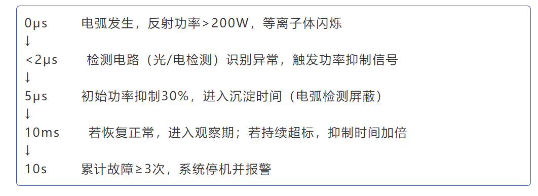
This process relies on the dual mechanism of “rapid response (<2μs) + tiered protection (suppress-recover-shutdown).” For example, the Taisman high-voltage power supply uses active filtering technology to reduce total harmonic distortion (THD) from 8.2% to <1.5%, with a 90% reduction in abnormal discharge rates; Advanced Energy’s Apex series RF generators integrate “high-speed arc management” functions, combined with factory-certified components replaced during refurbishment, significantly reducing fault recurrence rates.
In summary, the management of arc faults must encompass the entire chain of “detection-response-repair-optimization,” minimizing their impact on wafer yield through microsecond-level response speeds and systematic protection designs.
2. Excessive Reflected Power
Excessive reflected power is a typical fault in semiconductor RF systems, with the core cause being impedance mismatch—that is, the output impedance of the RF power supply cannot achieve conjugate matching with the load (such as the plasma process chamber), leading to ineffective energy transmission and reflection back to the source.
This mismatch can cause energy waste, potential equipment damage, and decreased substrate processing consistency, severely affecting process stability.
The following analysis of its causes from hardware, process, and system levels proposes corresponding progressive solutions.
1. Causes
(1) Hardware Level: Physical mismatches caused by passive component failures.
Degradation or failure of key components in the RF transmission link is a direct trigger for impedance mismatch. Typical issues include:
Vacuum capacitor jamming:
Moving plate bearings lacking lubrication or sintering due to arcing prevent the capacitor value from being adjusted, destroying the tunability of the matching network.Inductor performance degradation: Moisture or aging of the insulation layer causes the Q value to drop sharply from the design value (e.g., 200) to below 50, deviating from design parameters.Power supply and cable faults: Damage to internal modules of the RF power supply (e.g., RF faults) or poor contact of transmission cables directly leads to output impedance deviating from the standard 50 ohms..
(2) Process Level: Time-varying mismatches caused by dynamic characteristics of plasma.
The nonlinear changes in plasma state are the main source of impedance mismatch during the process:
E-H mode conversion anomalies: Failure of energy coupling mechanisms during the plasma ignition phase leads to sudden changes in load impedance, commonly seen in low-pressure (mTorr) processes..Pulse plasma reactance fluctuations: In pulsed mode (frequency >1kHz), plasma reactance changes rapidly with the pulse period, making it difficult for the bias power supply to couple, significantly increasing reflected power..Process chamber impedance drift: After long-term operation, deposition on chamber walls or changes in gas composition lead to nonlinear shifts in impedance over time, while the output impedance of the RF generator remains constant, exacerbating the mismatch..
(3) System Level: Systemic mismatches caused by matching mechanism defects.
The insufficient response capability of traditional matching systems is a deep-rooted reason for the persistent mismatch:
Static matching limitations: Matching networks with fixed capacitor values cannot adapt to dynamic changes in load impedance (such as fluctuations in plasma process conditions), leading to failure to lock or oscillate at the matching point..Scanning tuning delays: Traditional matchers find matching points through scanning, which is time-consuming and prone to missing dynamically changing matching points, especially prominent in multi-power level pulsed scenarios..
2. Progressive Solutions
To address the above causes, a comprehensive solution must be constructed from hardware maintenance, parameter optimization to system upgrades:
(1) Hardware Maintenance: Restore inherent performance of components.
Vacuum capacitor repair: Use ultrasonic cleaning to remove contaminants from bearings, and apply perfluoropolyether vacuum grease for lubrication to ensure smooth adjustment of the moving plate..Inductor coil refurbishment: Rewind the coil after stripping paint, using ceramic slurry impregnation treatment to enhance voltage resistance to 10kV, restoring Q value to above 200..Link detection: Regularly use network analyzers to test the standing wave ratio (VSWR) of RF cables, replacing aging connectors to ensure stable transmission link impedance..
(2) Parameter Optimization: Dynamically adjust impedance matching.
Real-time calibration of adjustable components: Adjust the tunable capacitors/inductors in the main line through the impedance matcher to make the input impedance of the matcher equal to the output impedance of the RF generator (usually 50 ohms), eliminating transmission line reflections..
Application of Automatic Matching Networks (AMN): AMN monitors load impedance changes in real-time, dynamically adjusting capacitor/inductor values through motor control to achieve conjugate matching between the power supply and load, with response speeds reaching microsecond levels..
Key optimization indicators: The ratio of reflected power to preset RF power must be controlled below 1%; for example, the maximum reflected power threshold for a certain model 500W RF generator is 200W, and in actual operation, the AMN must stabilize reflected power within 5W (1%×500W)..
(3) System Upgrades: Build an intelligent matching architecture.
Dual-frequency matching technology: Use a combination of 60MHz + 2MHz dual-frequency power supplies to enhance plasma density uniformity at high frequencies and optimize ion energy distribution at low frequencies, reducing impedance fluctuations at a single frequency.
Variable frequency collaborative matching: Combine variable frequency generators to dynamically adjust RF frequency within the pulse period, assisting impedance matching, especially suitable for multi-power level switching scenarios..Intelligent detection and control: Integrate the first detection unit (input side) and the second detection unit (output side), using AI algorithms to predict trends in impedance changes, adjusting matching parameters in advance, improving matching speed by over 30% compared to traditional solutions..
In actual maintenance, it is also necessary to combine fault isolation and preventive measures: Use system operation logs and environmental data to locate potential risks such as overheating, regularly check the status of ICP RF sources and RF systems, and establish preventive replacement strategies for vulnerable components like optocouplers and capacitors, which can significantly reduce the occurrence of power instability..
Welcome to join the semiconductor equipment and process communication group.~Please add the editor and note your company+Name+Position.
 Disclaimer: The content of this article comes from the public account (Semiconductor Pony), and this article is only for organizing and promoting semiconductors.