Thermal stress is a type of mechanical stress generally caused by temperature changes that prevent an object from expanding or contracting freely, resulting in internal stress within the object. When an object is subjected to external constraints or internal parts are mutually restrained, factors such as temperature gradients, restricted thermal expansion and contraction of materials, or thermal shock can lead to the formation of thermal stress. Common phenomena of thermal stress in daily life include: train tracks without expansion joints deforming due to thermal stress in summer, and glass shattering due to rapid heating and cooling.
The Importance of Thermal Stress on Substrates
For PCB substrates (copper-clad laminates), thermal stress specifically refers to the thermal stress generated in PCB substrates when exposed to high temperatures during the soldering process. In severe cases, this can lead to delamination of the surface copper foil from the resin substrate, or even separation between substrate layers. On one hand, most PCBs need to withstand multiple reflow soldering cycles, with the peak temperature of lead-free processes reaching 260°C; on the other hand, during multilayer board lamination, the substrate may undergo multiple high-temperature laminations. During these processes, the substrate must not experience structural failures such as delamination due to thermal stress. Therefore, to assess the substrate’s capability, we need to conduct thermal stress experiments.
Thermal Stress Experiments
In the production of high-frequency board products, thermal stress experiments are a mandatory inspection item for each batch quality check. This ensures that the substrate can still function normally in environments with drastic temperature changes, avoiding delamination or deformation due to thermal stress. In product development, extreme thermal stress experiments can identify potential defects in materials or manufacturing processes in advance, providing a basis for improving material selection, structural design, and manufacturing processes, thereby enhancing product reliability.
The thermal stress testing referred to in this article specifically denotes a testing method that simulates exposure to high-temperature environments during soldering to detect whether structural failures occur in the PCB substrate. Some literature refers to these tests as “thermal resistance experiments.” However, in a broader sense, thermal resistance experiments encompass a wider range of tests beyond thermal stress experiments. For example, the thermal delamination time experiments, pressure vessel thermal stress (GB/T 4722—9.1 section), and high-temperature oven baking thermal resistance experiments (GB/T 4722—6.12 section) introduced in our series of articles also fall under the category of thermal resistance testing methods for substrates.
The specific methods and standards for thermal stress testing of PCB substrates include: (1) IPC-TM-650 Test Method Manual 2.4.13.1 Thermal Stress of Laminates; (2) GB/T 4722-2017 Test Methods for Rigid Copper-Clad Laminates for Printed Circuits, Section 6.5, Thermal Stress; additionally, (3) IPC-TM-650 Test Method Manual 2.4.23 Solderability of Laminate Materials, and (4) IPC-TM-650 Test Method Manual 2.6.8.1 Thermal Stress, Laminates. Our company generally conducts tests based on the first two standards.
IPC-TM-650 2.4.13.1 primarily evaluates the thermal resistance of PCB substrates in high-temperature soldering environments, detecting defects such as delamination, bubbling, and copper foil peeling. The specific operational method is as follows:
Sample Preparation:
Sample Preparation:The number of samples is 3, randomly selected, with each sample measuring 2 inches by 2 inches. For double-sided copper-clad boards, both fully etched samples and samples retaining double-sided copper foil need to be prepared.
Sample Pre-treatment:Maintain in a ventilated oven at 125°C for 4-6 hours. Then store in a desiccator until cooled to room temperature.
Testing:
Sample Testing:The metal surface of the sample needs to be coated with flux (Rosin Flux). Then, place the sample on the surface of a molten tin bath, maintaining the temperature at a specific point (1 inch below the liquid surface) for 10 seconds. The specific temperature is not defined in IPC-TM-250 and national standards. Generally, the industry adopts 260°C (Method A) or 288°C (Method B). During this period, ensure close contact between the sample and the tin surface. Then remove the sample and lightly tap the edges to eliminate any excess solder. Visually inspect the sample for defects such as bubbling, delamination, or wrinkling. If necessary, metallographic sectioning can be performed for inspection.
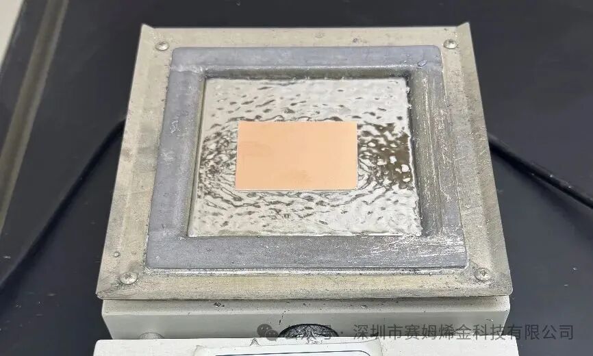
The above method is commonly referred to as solder float testing or floating solder testing. Additionally, GB/T 4722-2017 Section 6.5 and IPC-TM-650 Test Method Manual 2.4.23 describe another simulation method known as dip soldering or dip tin testing. The difference between the two is that dip tin involves immersing the test sample almost entirely in molten tin. Dip tin testing is very similar to the solderability testing in GB/T 4722-2017, Section 6.6, and IPC-TM-650 Section 2.4.12 Solderability, edge dip soldering method, but solderability testing focuses on the solderability of the copper foil surface of the copper-clad laminate. In dip tin testing, a special device or a clamp similar to tweezers holds one end of the sample, immersing the sample vertically below the surface of the solder. After the specified experiment, remove it, cool, and observe. Record any discoloration or surface contamination, softening, delamination, interlayer bubbling, lack of adhesive, white spots, cracking, or voids on the sample surface; for samples with copper foil, check for bubbling or delamination between the metal foil and the substrate.
According to the requirements of IPC-TM-650 and IPC-4103 standards, thermal stress tests for hydrocarbon copper-clad laminates and polytetrafluoroethylene copper-clad laminates generally test at 288°C for at least 10 seconds (based on Method 2.4.13.1). To more rigorously verify product reliability, our company extends the dip tin testing time for hydrocarbon high-frequency boards and polytetrafluoroethylene high-frequency boards to 60 seconds to simulate a more severe thermal stress environment, ensuring product performance stability under extreme conditions. Additionally, we also conduct thermal shock experiments simulating multiple soldering cycles, with 10 seconds of dip tin as one group, testing 6 groups. In product development, we generally conduct extreme tests, such as further increasing dip tin time or repeating tests on the same sample until failure occurs.
The results of thermal stress experiments on substrates are related to the substrate’s thermal expansion coefficient (CTE), glass transition temperature (Tg), mechanical strength, interlayer adhesion, bonding strength between copper foil and substrate, and the substrate’s moisture absorption properties. Once the substrate is processed into a PCB, thermal stress testing remains equally important. At this point, in addition to the stability of the substrate material itself, the processing technology is also a significant source of thermal stress failure in PCBs. Generally, thermal stress experiments for PCBs can be conducted according to the following sections in IPC-TM-650 Test Method Manual.
2.6.6 Temperature Cycling of Printed Circuit Boards
2.6.7 Thermal Shock and Connectivity of Printed Circuit Boards;
2.6.8 Thermal Stress, Coated Through Holes.
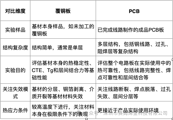
Differences Between PCBs and Substrates
Therefore, although both PCBs and copper-clad laminates involve thermal stress experiments, their respective focuses differ due to variations in structure, application scenarios, and failure modes. For example, the reliability of PCBs can be directly tested under real reflow soldering conditions, with set temperatures, transfer speeds, and cycle counts, making the testing more aligned with production conditions. Additionally, due to the relatively poor stability of densely positioned holes within the board, testing modules for densely positioned holes can be incorporated into the graphic design for thermal stress testing, focusing on the bubbling and delamination around densely positioned holes.
 ENDCompany Profile: Shenzhen Simenjin Technology Co., Ltd. (referred to as Simenjin Technology) is located in the Xin Qiao Comprehensive Building, Bao’an District, Shenzhen. The company’s R&D team has successfully developed graphene metallization technology and large-scale preparation technology for graphene used in circuit boards. In April 2018, the company established a production line for soft board graphene metallization in Shenzhen. In October 2019, the company established a production line in Dongguan City with an annual output of 50 tons of graphene slurry, which has been successfully put into production. The company gradually promotes the application of graphene metallization technology in circuit boards, electronic shielding, plastic electroplating metallization, pp film metallization, composite materials, and other fields of research and industrialization, striving to become a technological newcomer in the new energy and new materials industry within 3-5 years, using new technologies and new materials to transform related electronics and surface treatment industries, promoting environmentally friendly green technologies, reducing environmental pollution, and continuously advancing the technological progress and development of related industries.
Business Consultation Phone:
Mr. Chen:13823133110
Mr. Yang:13714337073
Company Landline:0755-23593156
Company Address:Beihuan Road, Xin Qiao Street, Bao’an District, Shenzhen