The appearance of “stair-step” or “irregular serrated edges” on PCB traces is usually not the intended design but rather a phenomenon that needs to be controlled, caused by a combination of manufacturing processes and physical principles. The core reason is the interaction between the edge effects of the photoresist layer (dry film or wet film) and the chemical reactions of the etching solution during the etching process. ★ Main Cause – “Lateral Etching” During the Etching Process This is the most direct reason for the formation of trapezoidal traces. 1. Review of the Production Process ♞ Film Application: A layer of photoresist dry film (or liquid photoresist) is applied to the copper-clad board. ♞ Exposure: The board is exposed to ultraviolet light through a film with circuit patterns. The exposed parts of the dry film undergo a chemical reaction, becoming less soluble in the developer. ♞ Development: The unexposed parts of the dry film are washed away, revealing the copper foil that needs to be etched. ♞ Etching: The board is placed in an etching machine, where the etching solution is sprayed to corrode the exposed copper. ♞ Stripping: The dry film protecting the traces is removed, resulting in copper traces.
2. Occurrence of “Lateral Etching” During the etching step, the etching solution not only corrodes the exposed copper vertically but also attacks the sidewalls of the copper traces horizontally. Ideally, etching should be perfectly vertical, but in reality, the etching solution can laterally etch from below the edge of the photoresist layer. The depth of this horizontal corrosion is referred to as the “lateral etch amount.”
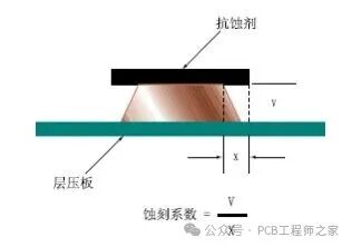
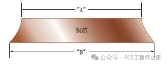
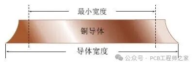
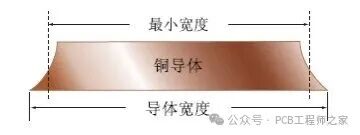
3. Formation of the Trapezoid Due to the protection of the photoresist layer, the copper directly above the trace is preserved intact. However, the copper below the edge of the trace is hollowed out by the etching solution from the side, forming an inwardly concave “pit.” Once etching is complete and the photoresist layer is removed, the cross-section of the trace is not an ideal rectangle but resembles a trapezoid or mushroom shape (if lateral etching is severe). From the top view, this lateral etching effect manifests as the edges of the traces no longer being straight lines but exhibiting small, irregular serrations or wavy shapes.
★ Factors Affecting the Degree of Lateral Etching1. Etching Method ✒︎ Immersion Etching: The worst effect, severe lateral etching, and rough edges. ✒︎ Spray Etching: The standard method in modern PCB factories. High-pressure spraying allows the etching solution to impact the board surface vertically, reducing the time the liquid stays on the sidewalls, thus mitigating lateral etching. The pressure, uniformity, and angle of the spray are critical. 2. Type and Condition of the Etching Solution ✒︎ Type: Different etching solutions (e.g., acidic, alkaline) have different etching characteristics and control capabilities over lateral etching. ✒︎ Concentration and Temperature: Low concentration or high temperature of the etching solution can lead to excessively fast and uncontrollable etching speeds, exacerbating lateral etching. ✒︎ Age: Overused etching solutions have reduced effective components and increased by-products (e.g., copper ions), which can decrease etching capability and uniformity, leading to more severe lateral etching and serrated edges.
Different controls yield different results, as shown in the following images:
3. Copper Foil Thickness The thicker the copper foil, the longer the etching time required, and the longer the etching solution attacks the sidewalls, naturally increasing the lateral etch amount. This is why fine traces typically use thin copper (e.g., 1/3 oz). 4. Quality of the Photoresist Layer ✒︎ Adhesion: If the adhesion of the dry film to the copper board is weak, the etching solution can easily “drill in” from the edges, leading to severe “plating” and lateral etching. ✒︎ Resolution and Thickness: The resolution of the dry film itself is limited, and it cannot perfectly present very fine lines. The thicker the dry film, the more pronounced the “eave” effect at the edges of the pattern, providing more space for lateral etching. ★ Why Control Trace Width and Bottom?1. Impedance Control
In high-frequency circuits (e.g., RF, high-speed digital signals), the transmission of signals is very sensitive to the geometric shape of the traces. A trapezoidal cross-section alters the characteristic impedance of the traces, leading to signal reflection, distortion, and decreased integrity. Models need to be used during design to compensate for this effect. 2. Current Carrying Capacity
Lateral etching reduces the effective cross-sectional area of the traces, thereby decreasing their capacity to carry high currents. 3. Limits of Fine Trace Processing
When the spacing between traces (width/spacing) is very small (e.g., below 3/3 mil), severe lateral etching may cause the lateral etching areas of two adjacent traces to connect, resulting in a short circuit. The fundamental reason for PCB traces exhibiting “stair-step” edges is the inevitable phenomenon of “lateral etching” during the etching process. This is a metric directly related to manufacturing process capability. By optimizing etching parameters, maintaining etching equipment, and selecting appropriate materials and chemicals, the lateral etch amount can be controlled to a minimum (usually only a few microns), resulting in smooth edges and nearly vertical traces.
This public account will continue to update PCB/FPC design and manufacturing related content, please “follow” to avoid missing the content you need…
If this has been helpful to you, please bookmark➕share➕like, thank you!
Previous Exciting Content:
Segmented Gold Finger Production Process and Control
PCB Impedance Matching and Software Calculation
Current/Resistance/Capacitance/Inductance Calculation
Rigid-Flex PCB Issues and Solutions
Analysis of PCB Manufacturing Defects and Causes
Common PCB Design DFM Traps
Basic Knowledge of PCB Materials (2)
Basic Knowledge of HDI (1)
Analysis of PCB Manufacturing Defects and Causes
Basic Knowledge of Back Drilling
Interpretation of IPC-4103 High-Speed High-Frequency Materials
At the request of everyone, a PCB technology exchange group has been established; feel free to join if needed…