
Click the blue text above to follow for more exciting content.
This article contains 898 words, and it takes about 3 minutes to read.
The full name of FPGA in Chinese is 现场可编程门阵列 (Field Programmable Gate Array), which is a special type of logic chip. Unlike other logic chips, users can define its hardware functions at any time. Invented in 1985 by Xilinx founder Ross Freeman, it is a logic chip with programmable characteristics that is pre-designed on a silicon wafer. The name FPGA reflects its characteristics at the time of its inception:1) Field-Programmable: In the 1980s, the configuration of chips was mostly stored in mask ROM or PROM (the basic settings or executable program code required at startup were permanently written into the mask ROM or PROM during manufacturing or configuration, ensuring that the chip could operate according to the predetermined configuration without external intervention). Changing the chip’s functionality required removing the chip and returning it to the wafer factory for modification, known as “Mask-programmable.” FPGA allows customers to configure the FPGA locally or remotely after receiving the chip, thus achieving configuration in the “field” where it is used.Programmable means that the wiring and logical layout of the FPGA’s underlying logic operation units are not fixed, allowing for the implementation of any digital logic function. While CPUs and GPUs can also be programmed, this programming refers to changing the configuration of their registers (the hardware structure of the registers is fixed, but their operations can be controlled and modified by writing programs), and users cannot change their hardware functions. In contrast, FPGA is hardware programmable, allowing users to configure internal logic blocks, wiring, I/O, and other resources, enabling the same FPGA to perform channel coding functions in a 5G base station and, after reconfiguration, to control motors in CNC machines. Therefore, FPGA is also known as the “universal” chip.2) Gate Array: FPGA is considered an “array” of gates, where the chip can be configured like a blank canvas to implement circuits with different functions. At the same time, gate arrays were the competitive products that FPGA was benchmarked against at its inception, being a customizable ASIC (the gate array design technology emerged in the early 1980s as a rapid automation design technology for application-specific integrated circuits (ASICs), utilizing pre-designed logic gate units and automated wiring technology to accelerate the ASIC design process), but only the wiring is modifiable, while the fixed transistors are pre-placed and cannot be changed, whereas FPGA allows both logic units and wiring to be repeatedly modified. Gate arrays were widely used in complex electronic systems with millions of gates in the 1990s, while the logic gate count of FPGA at that time generally did not exceed 250,000 gates. As the complexity of electronic systems increased, the architecture of gate arrays became increasingly redundant, while the LUT (Look-Up Table) based FPGA architecture became more streamlined and better suited for high-density designs. Therefore, by the end of the 1990s, FPGA quickly replaced gate arrays after breaking through the million-gate limit. (In other words, FPGA is a more advanced and flexible programmable logic device developed based on early programmable logic device technologies such as gate arrays.)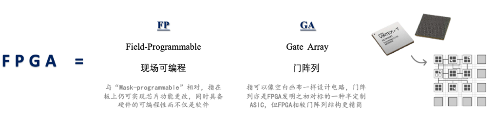 Appendix:
| Term | Definition | Main Features |
|
ROM (Read-Only Memory) |
It is a type of non-volatile memory, meaning it can retain stored data even without power supply. |
Non-volatile: ROM can stably store data and will not lose information due to power outages. Read-only: The data in ROM is written during manufacturing and cannot be modified by users during subsequent use. This feature makes ROM particularly useful for storing fixed programs or data. High integration: ROM has a high degree of integration, with fast read times, typically 20-50ns. |
|
Mask ROM |
The most basic type of ROM, where data is directly written into the chip during manufacturing and cannot be changed after leaving the factory. |
Low cost: Suitable for mass production, as the data is determined during manufacturing. |
|
Programmable Read-Only Memory (PROM) |
Allows users to write data in a specific way after manufacturing, but cannot be modified after writing. |
One-time programming: PROM chips are written once during manufacturing, and users cannot modify or erase the data. This feature makes PROM very suitable for storing programs or data that do not need to be modified. High stability: Since the data in PROM cannot be changed once written, the stored programs or data have high stability and security. This is particularly important for applications that require ensuring that the code is not modified. Security: The irreversibility of PROM makes it particularly important in security applications where data integrity must be ensured, such as in payment systems and secure boot programs. |
|
Register |
It is a high-speed, small-capacity storage unit within the computer’s central processing unit (CPU), used to temporarily store data, instructions, or other information. It serves as an important bridge between the CPU and memory, significantly accelerating data transfer and processing speed. |
High speed: Registers are located within the CPU and consist of high-speed flip-flops, so access speed is very fast, with almost no access delay. Small capacity: Despite the fast access speed, registers have relatively small capacity, typically storing only a small amount of data or instructions. This design balances speed and capacity. Diverse types: The CPU typically contains various types of registers, each with specific purposes and functions. For example, the accumulator (ACC) is used to temporarily store the results of arithmetic logic unit (ALU) operations; the instruction register (IR) stores the currently executing instruction; and the program counter (PC) indicates the address of the next instruction, etc. Programmability: Although the hardware structure of registers is fixed, their operations can be controlled by writing programs. Programmers can read, write, or modify the contents of registers by writing instructions to achieve specific data processing and control logic. |
|
Gate |
In electronics and integrated circuits, a gate refers to a logic gate, which is the basic unit that constitutes digital circuits and is used to perform basic logical operations. Logic gates generate output signals by controlling combinations of input signals and are the foundation of complex digital circuits. |
Basic logical functions: Gate circuits can perform basic logical operations such as AND, OR, NOT, and complex logical operations formed by combinations of these basic operations. Input and output: Gate circuits have one or more input terminals and one output terminal, with input signals processed through logical operations to produce output from the output terminal. Logic levels: The input and output signals of gate circuits are typically digital signals, i.e., high level (usually logic 1) and low level (usually logic 0). High integration: Modern integrated circuits often have gate circuits that are highly integrated, allowing complex logical functions to be implemented on a very small chip area. |
|
Gate Count |
Gate count refers to the number of logic gates on a chip. Logic gates are the most basic electronic components in a chip, used to perform logical operations. The number of gates on a chip directly determines its complexity and functionality. (Focus is on the number of logic gates) |
Affects circuit performance: The more gates there are, the greater the delay in signal transmission within the circuit, which may lead to a decrease in circuit operating speed. Design complexity: As the gate count increases, the complexity of circuit design also increases, requiring more resources and time for design and verification. Power consumption issues: Circuits with a high gate count may generate more power consumption during operation, especially noticeable at high frequencies. |
|
Gate Array |
A gate array is a semi-custom integrated circuit design method prepared by semiconductor manufacturers, where a motherboard with basic logic gates is formed on a silicon wafer. These logic gates are arranged in an array but are not pre-connected into specific circuits. Users can wire according to their desired circuit to form the required circuit structure on the motherboard. (Focus is on the layout and wiring of logic gates) |
Flexibility: Gate arrays allow users to wire on existing basic logic gate unit motherboards to form the desired circuits. This flexibility makes gate arrays adaptable to various application needs. Shortened production cycle: Since gate arrays use a common motherboard, they can significantly shorten production time and reduce production costs. Wide application: Gate arrays are widely used in various fields, including consumer devices such as digital cameras and DVD recorders, as well as industrial devices such as robots and CNC machines. Technical classification: Gate arrays can be divided into channel and non-channel types. Channel gate arrays leave fixed channel areas for wiring between gate units, while non-channel gate arrays use gate sea technology to wire in unused effective device areas, increasing circuit integration density. |
|
LUT (Look-Up Table) |
LUT is essentially a table or array that maps inputs to outputs. It allows for quick retrieval of results for complex calculations or transformations through simple lookup operations, without performing complex calculations. |
In FPGAs and other programmable logic devices, LUTs are one of the basic logic units. LUTs in FPGAs typically contain a certain number of inputs (e.g., 4, 5, or 6) and one output. Each LUT can be configured to perform any logical function from input to output. By pre-calculating and storing all possible input combinations corresponding to output values, LUTs can provide the required logical results within a single clock cycle, thereby improving the speed and efficiency of the circuit. |
|
ASIC (Application-Specific Integrated Circuit) |
It is an integrated circuit designed specifically according to application requirements. |
Custom design: ASIC is optimized for specific functions or application scenarios to achieve the best performance and power consumption. High performance: Since ASICs are custom-designed, they typically provide higher performance than general-purpose microprocessors or memory. Low power consumption: Through optimized design, ASICs also have significant advantages in power consumption. High cost: The design and manufacturing costs of ASICs are relatively high because they require custom development for specific applications. This high cost makes ASICs more suitable for applications with large-scale production. Application fields: ASICs have a wide range of applications, including communications, consumer electronics, medical, automotive electronics, aerospace, etc. In the IT field, ASICs are mainly used for high-speed data processing, data encryption, compression, and decompression tasks. |

Risk Warning:This content only represents the analysis, speculation, and judgment of the Breaking Research team, and is published here solely for the purpose of conveying information, not as a basis for specific investment targets. Investment carries risks; please proceed with caution!Copyright Statement:This content is copyrighted by the original party or author. If reproduced, please indicate the source and author, retain the original title and ensure the integrity of the article content, and bear legal responsibilities such as copyright.
END
