Proteus – Simulation of Programmable Logic Devices
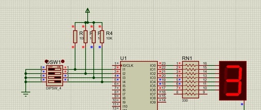
The goal of this example is to write a program for the AM22V10 type of Programmable Array Logic (PAL) circuit to simulate a decoder for a seven-segment display.To complete this project, you need to install the following software:WinCUPL which can be downloaded for free from the microchip website at https://www.microchip.com/en-us/development-tool/WinCUPL• The ISIS PROTEUS software from … Read more