Hello everyone, I am Pi Zi Heng, a serious tech enthusiast. Today, I will introduce the impact of Debug Mailbox implementation in i.MXRT600 on JLink debugging.
The story begins with my colleague, Ms. Kerry, who likes to dig deep into problems. She has been researching the i.MXRT600 chip and found that when connected to the chip’s USB port in ROM serial download (ISP) mode, the enumerated HID device (0x1fc9, 0x0020) can be seen normally in the device manager. This HID device can be used with the host tool blhost.exe for application program downloading. However, when using JLink to connect to the chip (selecting MIMXRT685, not CM33), the previous HID device disappears, and it seems like the chip has exited normal operation in ROM. This experience is quite different from that of the i.MXRT1050. Why is this happening? This is actually caused by the Debug Mailbox; let me explain:
1. Introducing the Debugging Issue
According to our previous debugging experience with the i.MXRT1050, after setting the chip to serial download mode and connecting it with JLink, halting the core results in the chip’s PC normally stopping in the ROM area (after 0x200000). Let’s perform the same process on the i.MXRT600:
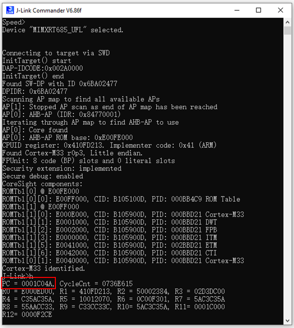
We found that the PC points to 0x1c04a, and no matter how you reset and halt again, it stays at this location. Strangely, this location is not in the ROM area (after 0x03000000 or 0x13000000). What is going on?
2. What is Debug Mailbox?
Unlike the i.MXRT1050, the i.MXRT600 introduces the Debug Mailbox mechanism, which is implemented by the ROM. Therefore, the behavior after connecting to JLink is determined by the Debug Mailbox mechanism.
Opening the i.MXRT600 User Manual, information regarding the Debug Mailbox can be found in the Debug subsystem chapter. The Debug Mailbox was originally a feature newly introduced in the NXP LPC series and later used in the i.MXRT600.
The following diagram shows the internal connection of the SWD debugging system in the i.MXRT600, where the blue box indicates the DM AP, which is the Debug Mailbox.
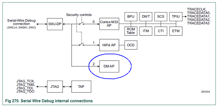
We know that the i.MXRT600 is an MCU based on the Cortex-M33 core, which features security. Therefore, NXP has incorporated many security features into the chip design, and the Debug Mailbox is one of them. The Debug Mailbox is based on NXP debug authentication protocol version 1.0, primarily serving to facilitate communication between external debuggers and the chip’s internal ROM, thus enabling functions like erasing Flash, entering ROM ISP, and debugging authentication.
3. Debug Mailbox Implementation in ROM
So what exactly is the Debug Mailbox mechanism in ROM? Simply put, it is a piece of code inserted into the ROM initialization process. This mechanism is quite simple; it ensures that the debug features are enabled and initializes the debug port based on the chip’s reset type, deciding whether to enter Mailbox command processing.
// Confirm that the debug feature is properly enabled in IFR
if (kStatus_DBG_Success != debug_auth_evaluate_dcfg_socu())
{
    __set_FAULTMASK(1);
    __WFI();
}
volatile uint32_t reset_status = RSTCTRL0->SYSRSTSTAT;
// Set initial debug port state based on reset type
if (kStatus_DBG_Success != debug_auth_hal_set_initial_debug_port_state(reset_status))
{
    __set_FAULTMASK(1);
    __WFI();
}
if (reset_status & 0x20)
{
    // Process commands received from the debugger
    debug_mailbox_GetRequest();
}
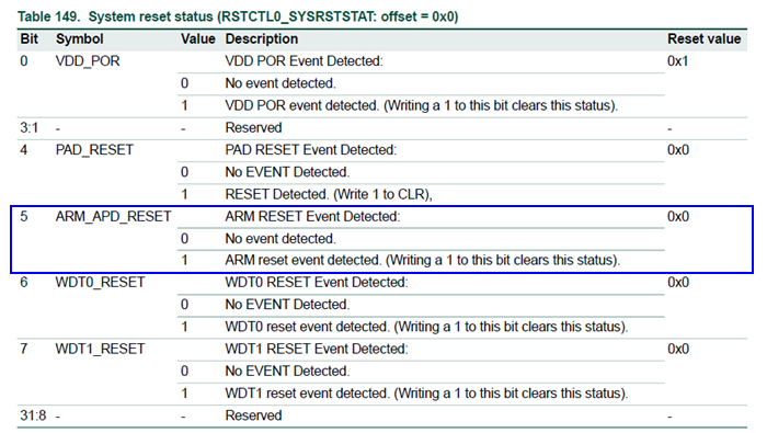
The RSTCTRL0->SYSRSTSTAT[5] bit indicates whether a warm reset occurred in the ARM core. During normal chip power-up, this bit will not be set to 1. However, if a debugger connects and issues a soft reset to the core, this bit will be set. Once this bit is set, the ROM initialization process will enter the Mailbox command processing function debug_mailbox_GetRequest(), and will not proceed with the normal ROM serial download/start process.
The debug_mailbox_GetRequest() function is the core of the Debug Mailbox mechanism. It interacts with the ROM using the following three Mailbox registers:
- CSW: Command Status Register, which the debugger uses to indicate to the ROM to enter mailbox command parsing state.
- REQUEST: Request Register, where the debugger writes mailbox commands to indicate the ROM to execute.
- RETURN: Result Register, from which the debugger reads to obtain the result of the mailbox command executed by the ROM.
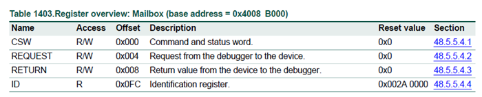
For users, typically, the debugger first writes 0x21 to the CSW register to request re-sync while resetting the device, and then writes specific commands to the REQUEST register as needed to achieve the corresponding functions of the Debug Mailbox.
#define ENTER_DEBUGGER_MAILBOX (0x0001)  // Start Mailbox debug
#define GET_CRP_LEVEL          (0x0002)  // Deprecated and return 3
#define DM_ERASE_FLASH         (0x0003)  // Mass erase flash
#define EXIT_DEBUGGER_MAILBOX  (0x0004)  // Exit Mailbox debug
#define ENTER_ISP_MODE         (0x0005)  // Enter specified ISP mode
#define SET_FA_MODE            (0x0006)  // Set to "Fault Analysis" mode
#define START_DEBUG_SESSION    (0x0007)  // Start Debug session
#define DEBUG_AUTH_START       (0x0010)  // Start Debug Authentication Protocol
#define DEBUG_AUTH_RESP        (0x0011)  // Debug Authentication response
4. JLink Script to Activate Debug Mailbox
Having understood the principles of the Debug Mailbox mechanism, let’s look at the Script content that must be loaded when connecting JLink to the i.MXRT600 (as mentioned earlier, MIMXRT685 must be selected, not CM33, because in the JLink DLL / JLinkDevices.xml, MIMXRT685 is the only one with a default Script specified). For knowledge about JLink Script, you can refer to my previous article “Basics of JLink Script Files and How to Call Them in IAR”.
This script content is actually provided in pseudocode in the i.MXRT600 User Manual, which uses JLINK_CORESIGHT_WriteAP() to write to the Mailbox registers (index 0 corresponds to CSW, index 1 corresponds to REQUEST), essentially following the Debug Mailbox usage process introduced earlier, and finally writing the START_DEBUG_SESSION command into the REQUEST register to enable the chip debugging mode.
void InitTarget(void) {
  int v;

  JLINK_CORESIGHT_Configure("IRPre=0;DRPre=0;IRPost=0;DRPost=0;IRLenDevice=4");
  // Pre-select that we have a Cortex-M33 connected
  CPU = CORTEX_M33;
  // J-Link is allowed to use a TAP reset for JTAG-chain auto-detection
  JTAG_AllowTAPReset = 0;

  JTAG_SetDeviceId(0, 0x6BA02477);

  // Read AP ID register to identify DM AP at index 2
  JLINK_CORESIGHT_WriteDP(2, 0x020000f0);
  v = JLINK_CORESIGHT_ReadAP(3);
  JLINK_SYS_Report1("DAP-IDCODE:", v);
  // Select DM AP index 2
  JLINK_CORESIGHT_WriteDP(2, 0x02000000);
  JLINK_CORESIGHT_ReadDP(0);

  // Activate DebugMailbox
  JLINK_CORESIGHT_WriteAP(0, 0x21);
  JLINK_CORESIGHT_ReadAP(0);

  // Enter Debug Session
  JLINK_CORESIGHT_WriteAP(1, 0x07);
  JLINK_CORESIGHT_ReadAP(0);
}
5. Status in Chip Debug Mode (REQUEST = 0x07)
As mentioned earlier, the JLink Script will put the chip into debug mode. So what is the status of the chip in debug mode? The ROM actually executes a small piece of code from 0x1c040 to 0x1c04B, ultimately stopping at 0x1c04a with while(1);, thus revealing the truth.
void go_debug_mode(void)
{
#define VECTOR_DUMMY_ROUTINE 0x0001c000u
#define APP_ENTRY (VECTOR_DUMMY_ROUTINE + 0x40 + 1)
    uint32_t dummy_loop_routines[] = {
        VECTOR_DUMMY_ROUTINE + 0x1000, // SP
        APP_ENTRY,                     // Reset Handler
        APP_ENTRY,                     // NMI Handler
        APP_ENTRY,                     // HardFault_Handler
        APP_ENTRY,                     // MemManage_Handler
        APP_ENTRY,                     // BusFault_Handler
        APP_ENTRY,                     // UsageFault_Handler
        APP_ENTRY,                     // SecureFault_Handler
        0,                             // Reserved
        0,                             // Reserved
        0,                             // Reserved
        APP_ENTRY,                     // SVC_Handler
        APP_ENTRY,                     // DebugMon_Handler
        0,                             // Reserved
        APP_ENTRY,                     // PendSV_Handler
        APP_ENTRY,                     // SysTick_Handler
        // Below are the binary codes for :
        //   register uint32_t dummy = SCB->CPUID;
        //   while(1);
        0x5000f64eu,
        0x0000f2ceu,
        0xe7fe6801u,
    };

    {
        uint32_t *dest = (uint32_t *)VECTOR_DUMMY_ROUTINE;
        uint32_t *src = (uint32_t *)&dummy_loop_routines[0];
        for (uint32_t i = 0u; i < ARRAY_SIZE(dummy_loop_routines); i++)
        {
            *dest++ = *src++;
        }
        jump_to_boot_image(VECTOR_DUMMY_ROUTINE);
    }
}
6. Impact of Debug Mailbox on JLink Debugging
Based on the above analysis, I will summarize the impact of the Debug Mailbox on JLink debugging:
- When the chip is executing in ROM (e.g., in ISP mode or if there is no application program in Flash), JLink must load the script to enable chip debugging mode; otherwise, it will not connect to the chip.
- After successfully connecting to the chip by loading and executing the JLink Script, the PC always stops at 0x1c04a, which is determined by the Debug Mailbox mechanism.
- Only when the chip normally starts the application program in Flash (i.e., exits ROM), can JLink connect to the chip (selecting CM33, without loading the script), and halting the core will point the PC to the actual application program location.
Thus, I have introduced the impact of the Debug Mailbox implementation in the i.MXRT600 on JLink debugging. Where is the applause~~~