1. Constraint Files
There are three types of constraint files in Xilinx ISE FPGA design: User Constraint File (.UCF), Netlist Constraint File (.NCF), and Physical Constraint File (.PCF). These can achieve timing constraints, pin constraints, and area constraints.
Users write UCF files during the design input phase, then the UCF file generates the NCF file after synthesis, and finally, the PCF file is generated after implementation.
The UCF file has the highest priority.
2. Syntax Description of UCF Files
(1) Syntax
The syntax of a UCF file is as follows:
{NET|INST|PIN} “signal_name” Attribute;
Where,
“signal_name” refers to the name of the constrained object, which includes the description of the object’s hierarchy;
“Attribute” is the specific description of the constraint; the statement must end with a semicolon “;”. Comments can be added using “#” or “/* */”.
It is important to note: UCF files are case-sensitive, and the signal names must match the case used in the design, but the constraint keywords can be uppercase, lowercase, or mixed case. For example:
NET “CLK” LOC = P30; # Purpose: Assign the CLK signal to pin P30 of the FPGA.
“CLK” is the constrained signal name. LOC = P30 is the meaning of the constraint.
For all constraint files, using the same signal name as the constraint keyword or reserved words in the design environment will generate an error message unless enclosed in ” “. Therefore, it is best to enclose all signal names in ” ” when inputting constraint files.
(2) Wildcards
In UCF files, wildcards refer to “*” and “?”. “*” can represent any string and empty, while “?” represents a single character. When editing constraint files, using wildcards can quickly select a group of signals, provided these signals share a common substring. For example:
NET “*CLK?” FAST; # Purpose: To select all signals that contain the “CLK” character and end with one character, enhancing their speed.
In positional constraints, wildcards can be used in row and column numbers. For example:
INST “/CLK_logic/*” LOC = CLB_r*c7; # Purpose: Place all instances in the CLK_logic hierarchy in the 7th column of the CLB.
(3) Defining Design Hierarchy
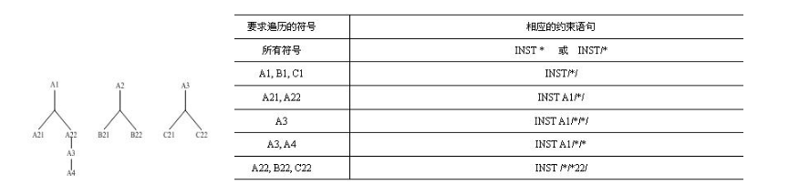
In UCF files, the wildcard * can specify the design hierarchy of signals. The syntax rules are:
* Traverse all levels
Level1/* Traverse modules in level1 and below
Level1/*/ Traverse modules in level1 but not lower-level modules
Example 4-5: Using wildcards to traverse the modules required in Table 4-3 based on the structure shown in Figure 4-75.
3. Pin and Area Constraint Syntax
LOC constraints are the most basic placement and synthesis constraints in FPGA design, defining the positions of basic design units on the FPGA chip, allowing for absolute positioning, range positioning, and area positioning. Additionally, LOC can constrain a group of basic units within a specific area. LOC statements can be written in constraint files or directly added to design files. In other words, the main functions of the FPGA Editor, Floorplanner, and pin and area constraint editor in ISE can all be accomplished through LOC statements.
(1) LOC Statement Syntax
The basic LOC syntax is as follows:
INST “instance_name ” LOC = location;
Where “location” can be any one or more valid locations on the FPGA chip. If multiple locations are specified, they should be separated by commas “,” as follows:
LOC = location1,location2,…,locationx;
Currently, placing multiple logic elements at the same location or placing multiple logic elements at multiple locations is not supported. It should be noted that multi-location constraints do not place the design at all specified locations, but rather allow the placer to randomly select one as the final placement location during the layout and routing process.
The syntax for range positioning is:
INST “instance_name” LOC=location:location [SOFT];
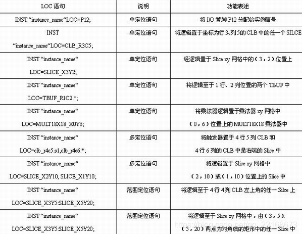
Common LOC positioning statements are shown in Table 4-4.
When defining ports using LOC, the syntax is as follows:
NET “Top_Module_PORT” LOC = “Chip_Port”;
Where “Top_Module_PORT” is the signal port of the top-level module in the user design, and “Chip_Port” is the pin name of the FPGA chip.
There is a priority in LOC statements; when both LOC ports and their connecting wires are specified, the priority of the wire constraint is the highest. For example, in Figure 4-76, LOC=11 has a higher priority than LOC=38.
LOC Priority Diagram
(2) LOC Attribute Description
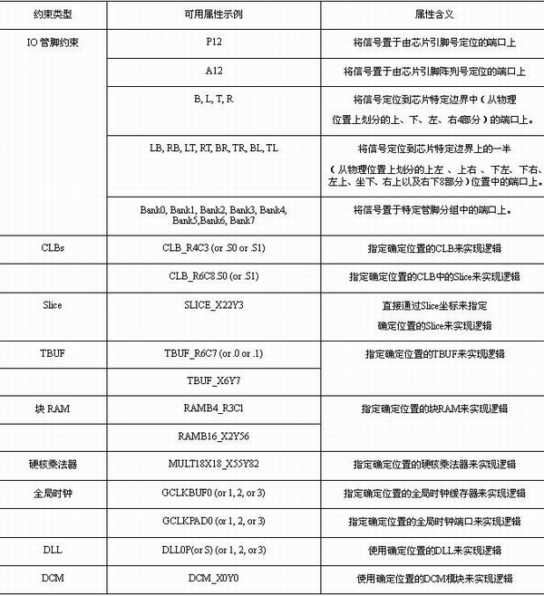
LOC statements can constrain pin locations, CLBs, Slices, TBUF, Block RAM, hard multipliers, global clocks, Digital Clock Managers (DCM), and other resources by loading different attributes, covering almost all types of resources in an FPGA chip. Thus, the LOC statement is very powerful, and Table 4-5 lists the commonly used attributes of LOC.
Original link: https://blog.csdn.net/qq_22168673/article/details/102956995
Recommended training class for FPGA employment at ZhiXin Technology—helping you step into success, break through yourself, and challenge high salaries. Classes start on April 20 in Beijing, welcome to consult for a trial! Common communication methods between FPGA and upper computers, common simulation knowledge in Verilog HDLScan to add WeChat and invite you to join the FPGA study group

Welcome to join the FPGA WeChat study group at ZhiXin Technology, where there are excellent FPGA engineers, students, and teachers. This is a strong atmosphere for FPGA technology exchange and learning, sharing and helping each other. Invite your friends to join!
Click to view your best look