Hello everyone, I am Sanshi. Previously, we learned about the parallel use of high-power power supply MOSFETs, today we will discuss the core points of Buck circuit PCB layout.
Generally speaking, the most important aspect of a Buck circuit is
Power Circuit Layout: The Top Priority
The power circuit is the core path that carries large currents and performs energy conversion. Its layout directly determines the stability, efficiency, and electromagnetic interference (EMI) level of the power supply.The routing of the power circuit should be asshort as possible, and the traces should be as wide as possible to reduce parasitic inductance and resistance, thereby lowering power loss and voltage noise. At the same time, it is essential to maintain the minimumloop area to suppress electromagnetic noise radiation.
When a synchronous Buck circuit operates, there are two modes of current: the upper switch is on (inductor charging)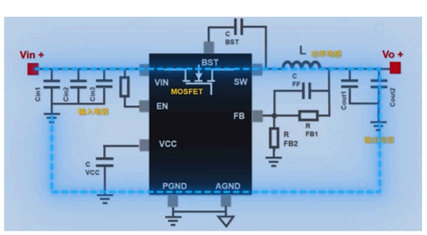 the upper switch is off (inductor discharging) current loop
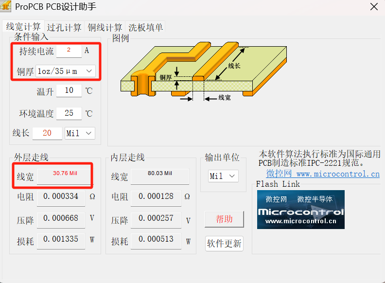
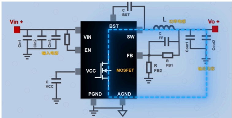 This two loops are key optimization targets.Key Component Layout Points:Input Capacitor (CIN) Location: Must be placed close to the chip’s VIN and power ground (PGND) pins.Reason: Input current is discontinuous, and parasitic inductance can cause severe noise. Placing it nearby provides a low-impedance path to absorb noise and serves as energy storage. It is recommended to keep the distance less than 40 mil (about 1 mm).Switch Node (SW) Characteristics: This is the node with high-speed voltage transitions and is the main source of noise.Design Points: The copper area should be as small as possible while ensuring current-carrying capability to reduce the antenna effect. Routing should be kept away from sensitive weak signal lines (such as feedback circuits). For high current applications, avoid vias at the SW node to prevent noise coupling to other layers.Output Capacitor (COUT) Location: Needs to be placed close to the output terminal (VOUT) of the inductor and power ground (PGND).Reason: Similar to the input capacitor, the goal is to minimize the power circuit. PGND should be connected to the output capacitor with short and wide copper traces.Copper Pour and ViasCopper Pour: The copper pour for VIN, VOUT, and GND should be maximized to reduce parasitic impedance and enhance current-carrying and heat dissipation capabilities. SW copper pour needs to balance current-carrying and noise.Vias: A large number of vias are needed in the VIN, VOUT, and GND networks to provide sufficient current-carrying capacity and good heat dissipation paths. The number of vias and trace width can be estimated based on software current (for example, with a temperature rise of 10℃, via inner diameter 0.25mm, maximum 1A. Trace width 30.76 mil 1OZ copper, maximum current 2A).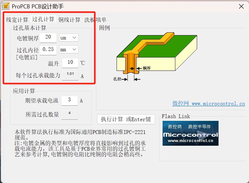
Logic and Control Circuit Layout:
This part of the circuit is responsible for controlling signal transmission, operates at low voltage, and is susceptible to interference, requiring a “clean” layout.
Bootstrap Circuit (BST) Function: Used to drive the gate of the integrated upper switch (NMOS) to a voltage higher than the SW point.Layout: The bootstrap capacitor must be placed close to the chip’s BST and SW pins. Since the BST node is also a high-speed switching node that radiates noise, the routing length must be strictly controlled (usually 20 mil wide is sufficient) to prevent interference with other circuits.Feedback Circuit (FB) Importance: This is the most sensitive part of the entire system. The voltage at the FB pin is usually very low (0.6-0.8V) and is easily affected by noise, which is a common cause of system instability.Layout: The voltage divider resistors and feedforward capacitors should be placed as close as possible to the chip’s FB pin.FB routing should be as short as possible to minimize parasitic parameters.FB routing should be kept away from noise sources, such as SW, inductors, BST, etc. If layer changes are necessary, this principle should still be followed.VCC Decoupling Capacitor Function: Provides power and voltage stabilization for the chip’s internal logic circuit.Layout: Should be placed close to the chip’s VCC and GND pins, preferably on the same layer as the chip to avoid using vias.Among these, it is most important to maintain the loop area, paying attention to inductance and feedback points. If the manual has layout specifications, it is advisable to refer to the manual for circuit layout planning.
Software Resource Acquisition
Follow the public account: Sanshi Electronics Room, and send the corresponding download keyword in the public account to obtain the link
Keyword: Download PCB Assistant
It is recommended to copy and paste O(∩_∩)O
Disclaimer:
This account maintains neutrality regarding all original and reprinted articles’ statements and views. The articles pushed are for readers’ learning and communication only. The copyright of articles, images, etc., belongs to the original author. If there is any infringement, please contact for deletion.