The PCIe bus is designed as an evolution of the PCI bus, and understanding the PCIe bus begins with learning about PCI. The birth of the PCI (Peripheral Component Interconnect) bus is closely related to the rapid development of PCs (Personal Computers). In processor architecture, the PCI bus is categorized as a local bus. The local bus serves as an extension of the system bus, primarily connecting external devices.
Unlike previous IO buses, PCIe uses a serial, point-to-point interconnect method to achieve communication between two devices, sharing similarities with traditional PCI and PCI-X. PCIe maintains the same memory, IO, and configuration address space model as traditional PCI, ensuring backward compatibility with legacy PCI systems.
The diagram below illustrates the various PCIe interconnections in a PC: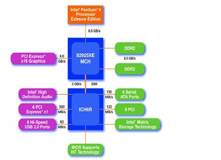
1. Overview of PCI Architecture
The platform based on the PCI bus is shown in the diagram below:
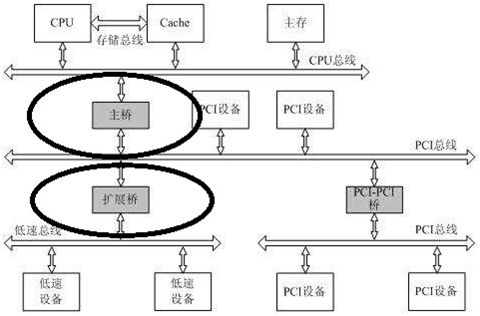
This platform mainly consists of FSB, PCI, and ISA, where FSB is the processor subsystem bus, PCI bus, and ISA is various IO expansion buses. In the image, circle 1 represents the northbridge (main bridge), and circle 2 represents the southbridge (expansion bus bridge).
2. PCI Bus Signals and Functions
The PCI bus signals are illustrated in the diagram below:

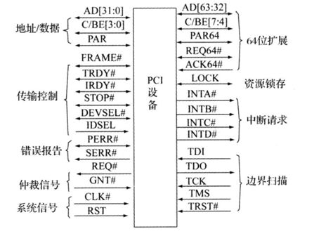
The signal functions are as follows:
-
Address/Data
AD[31:0]: Address and data multiplexed pins, usually sending the address first, followed by the data. It can represent a 32-bit physical address or 32-bit valid data.
C/BE[3:0]: Bus command and byte enable multiplexed pins, where during the address phase, it indicates the type of transaction on the bus; during the data phase, it indicates byte enables.
PAR: Parity bit for AD[31:0] and C/BE[3:0]#.
-
Transfer Control Signals
These signals mainly indicate the operational state of devices on the PCI bus. Based on their English meanings, their corresponding functions can be inferred. IDSEL is the PCI device configuration space chip select signal, used when the CPU accesses the PCI device for configuration.
-
Arbitration Signals
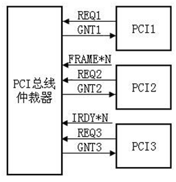
REQ#: The arbitration signal from the master device to the PCI device;
GNT#: The response signal from the slave device to the master device.
-
Error Signals
PERR: Reports data parity check for all PCI transactions outside of special scenarios;
SERR: Generally indicates three types of errors, including address parity check errors, data parity check errors, and other severe errors.
-
System Signals:
Includes clock signals and reset signals
-
Interrupt Signals:
-
64-bit Bus Expansion Signals
The bus expands from the previous 32-bit width to 64-bit, with a new set of signals added to accommodate this expansion.
3. Types of Transactions on the PCI Bus
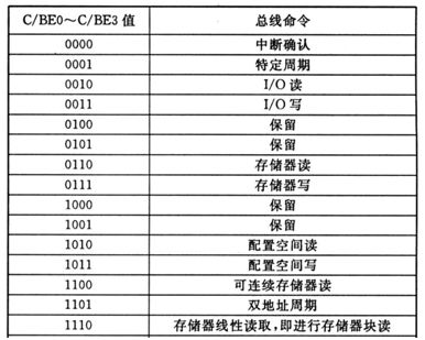
Based on the encoding of the signal C/BE[3:0], the types of transactions that PCI can perform are illustrated in the diagram below:
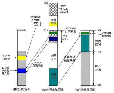
4. PCI Address Space Mapping
5. Typical PCI Read/Write Transactions
The diagram below illustrates a typical PCI read/write transaction, starting with an address phase, followed by a combination of one address phase and multiple data phases.
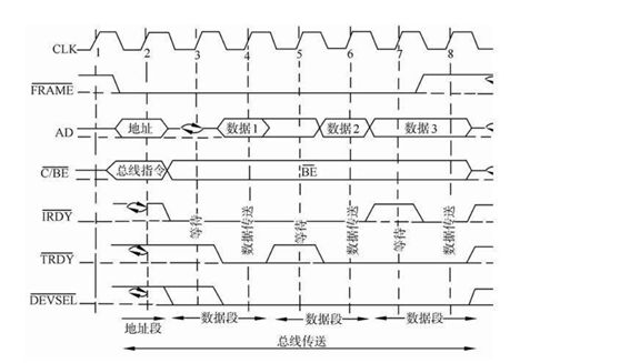
The master device indicates that this is the last data phase of the transaction during the final data phase when IRDY is asserted. The transmission of the last data depends on the TRDY signal.
6. Arbitration of the PCI Bus
7. PCI Header 0/1 Configuration Registers
The configuration registers serve as the handover area for information between the hardware of the PCI device and its initialization software and error handling software, reflecting the status and requirements of the PCI device in real-time.
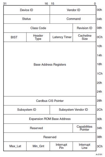
Since the register address width is not 32 bits, the concept of register number is introduced here.
8. Points IC Verification Engineers Need to Validate
l Validate different link speeds based on different versions of PCIe; PCIe link speeds are backward compatible (e.g., 3.0 supports 8G links, backward compatible with 2.5G and 5G).
l PCIe register access in different bidding areas;
l PCIe reset validation, including cold reset, hot reset, and warm reset.
l PCIe configuration validation, including IO, CFG, MEM, MSG validation;
l Determining the three packet formats of PCIe;
l Validation of the PCIe power management module, including validation of various states and state machine transitions;
l Whether the injection of malformed PCIe packets aligns with expectations;
l Validation of PCIe PHY (PCS and PMA) and DMA functions;
Some functionalities require validation through callbacks in VIP.


Detailed Introduction to IC Design Positions: “Digital Verification Engineer”
Detailed Introduction to IC Design Positions: “Digital Front-End Design Engineer”
Detailed Introduction to IC Design Positions: “Digital Back-End Design Engineer”
Detailed Introduction to IC Design Positions: “DFT Design Engineer”
Detailed Introduction to IC Design Positions: “Analog Layout Engineer”
Benefits
Reply with the keyword “Get Materials” to receive the IC material package.