“ This article introduces the key principles and practices for correctly routing USB differential data lines on a PCB. The main goal is to achieve the 90-ohm impedance matching specified in the USB standards, while also considering ESD protection and a complete ground plane.“
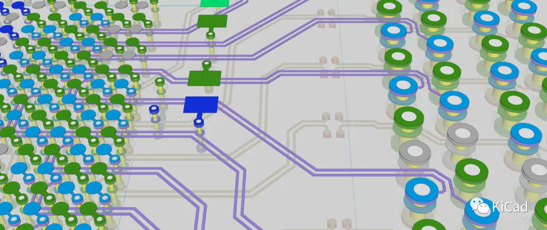 USB Speed Levels and Impedance Requirements
The USB speed standards have undergone multiple iterations, with significant differences in speed across different versions of USB interfaces. Below are the theoretical maximum transmission speeds for common USB standards:
| USB Version | Maximum Transmission Speed (Theoretical) | Common Name | Notes |
|---|---|---|---|
| USB 1.1 | 12 Mbps (1.5 MB/s) | Full Speed | Very old, basically obsolete |
| USB 2.0 | 480 Mbps (60 MB/s) | High Speed | Still widely used, relatively slow |
| USB 3.0 | 5 Gbps (625 MB/s) | SuperSpeed | Common in mechanical hard drives, USB flash drives |
| USB 3.2 Gen1 | 5 Gbps (625 MB/s) | SuperSpeed | Essentially a rebranding of USB 3.0 |
| USB 3.2 Gen2 | 10 Gbps (1250 MB/s) | SuperSpeed+ | Common in high-end USB flash drives, SSDs |
| USB 3.2 Gen2x2 | 20 Gbps (2500 MB/s) | SuperSpeed+ x2 | Requires dual-channel cabling |
| USB4 Gen2 | 20 Gbps (2500 MB/s) | USB4 20Gbps | Compatible with Thunderbolt 3/4 |
| USB4 Gen3 | 40 Gbps (5000 MB/s) | USB4 40Gbps | High-end laptops/external GPU docks |
For USB 1.1 and USB 2.0, the theoretical maximum speed does not exceed 480 Mbps, so while it is necessary to meet the basic differential pair routing constraints and 90-ohm impedance matching requirements, the layout requirements are not high, and meeting general constraints is usually sufficient. However, for USB 3.0 and above, the speed jumps from 480 Mbps to 5 Gbps, and the layout and routing requirements become much stricter, as high-speed signal lines are extremely sensitive to any physical imperfections on the PCB.
General USB Routing Constraints
First, remember the core principle: everything is for 90-ohm impedance.
The four main physical parameters that determine differential impedance are:
-
Trace Width: The wider the trace, the lower the impedance.
-
Trace Spacing: The closer the two traces are, the stronger the coupling, and the lower the differential impedance.
-
Dielectric Thickness (PP): The height of the trace above its reference plane (usually the GND layer). The farther away, the higher the impedance.
-
Dielectric Constant (Er): The characteristics of the PCB material. The most commonly used FR-4 material has an Er value typically between 4.2 and 4.6.
Therefore, to answer the question “How wide should the traces be, and how far apart?” you must first determine your PCB stack-up structure and then use impedance calculation tools (such as Polar Si9000, Saturn PCB Toolkit, Huaqiu DFM, or calculators provided by EDA software) to back-calculate the appropriate width and spacing.
Reference Values for Common Scenarios
Although there are no fixed values, in the industry, the most common4-layer boards, FR-4 materials, and standard stack-up designs do have some widely used “rules of thumb” or “starting values”. You can use these values as a starting point for your design and then fine-tune them based on your actual board manufacturer’s parameters.
Here are some reference values for typical scenarios (target: 90Ω differential impedance):
Scenario 1: Most Common 4-Layer Board (Signal-Ground-Power-Signal)
-
Stack-up: The dielectric thickness from the top layer (signal) to the second layer (ground) is typically between 6-8 mil (0.15-0.20 mm).
-
Copper Thickness: 0.5oz (17.5um) or 1oz (35um).
-
Common Combination 1:
-
Trace Width: 5 mil (approximately 0.127 mm)
-
Spacing: 7 mil (approximately 0.178 mm)
-
Common Combination 2:
-
Trace Width: 6 mil (approximately 0.152 mm)
-
Spacing: 6 mil (approximately 0.152 mm)
Scenario 2: Cases with Thicker Dielectric Layers
-
If the distance from the signal layer to the reference ground layer is thicker, such as 10-12 mil, to maintain 90Ω impedance, the traces need to be made wider.
-
Possible Combination:
-
Trace Width: 7 mil (approximately 0.178 mm)
-
Spacing: 6 mil (approximately 0.152 mm)
Best Practices and Recommendations
The above are just theoretical calculations; the most important step in practice is to communicate with the board manufacturer and request their recommended stack-up structure to obtain information on layer thicknesses, dielectric constants, etc., for precise impedance calculations.
Here is a recommended convenient method: use the impedance calculation tool in Huaqiu DFM. Since Huaqiu is also a board manufacturer, the DFM tool can directly access their commonly used stack-up information without the need to communicate with the manufacturer by phone or retrieve parameters from their website. The specific steps are as follows:
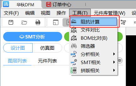
1. Open the impedance calculation tool in Huaqiu DFM:
2. Set the number of layers, board thickness, inner and outer copper foil thickness, and then select the type of glass cloth. This step is crucial, as the type of glass cloth determines many key parameters for impedance calculations.
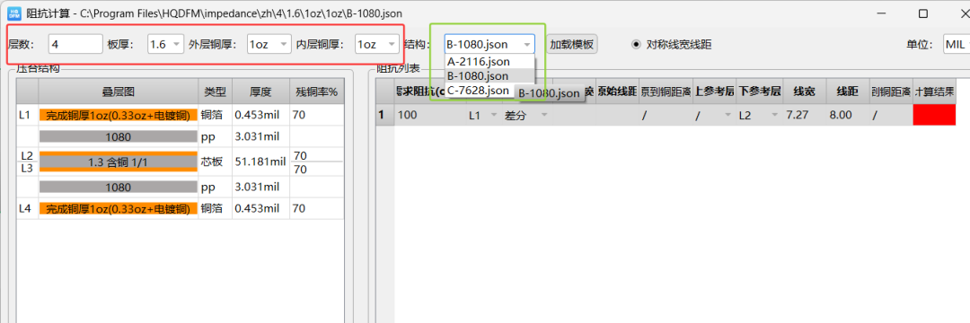
Below are commonly used glass cloth types.
| Glass Cloth Type | Nominal Original Thickness | Thickness After Lamination | Typical Dk@1 GHz | Memory Aid |
|---|---|---|---|---|
| 1080 | 0.075 mm | ≈ 65 µm | 4.2–4.3 | “Thinnest, 3 mil layer” |
| 3313 | 0.095 mm | ≈ 80 µm | 4.3 | “Common combination for high-speed boards” |
| 2116 | 0.105 mm | ≈ 90 µm | 4.4–4.5 | “Classic 4 mil, good impedance tuning” |
| 7628 | 0.185 mm | ≈ 170 µm | 4.6–4.7 | “7 mil thick, power/ground isolation” |
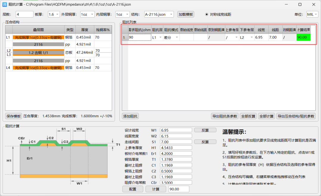
The biggest advantage of calculating impedance in Huaqiu DFM is that these stack-up structures are completely consistent with the stack-ups used by Huaqiu when manufacturing PCBs, eliminating communication issues. Additionally, once the type is selected, the parameters will automatically display in the impedance calculator without manual entry:
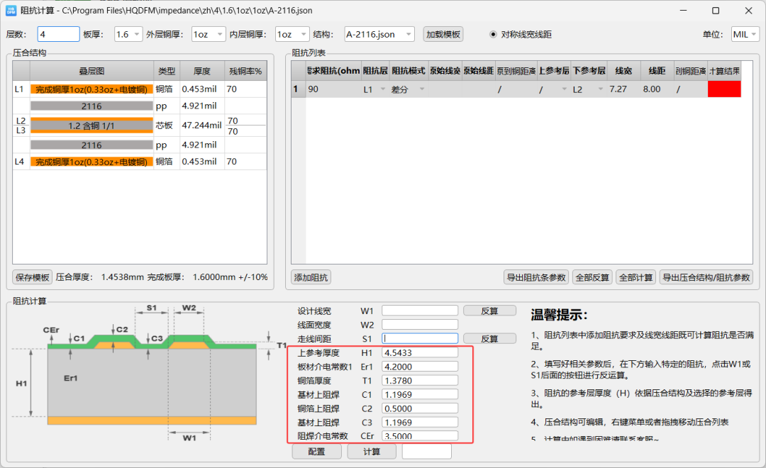
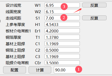
3. Input the target impedance of 90 ohms, assuming the trace spacing is set to 7 mil, click “Reverse Calculate” to obtain the trace width for the differential pair:
The results will automatically fill in the impedance list above for easy verification:
Ground Plane Requirements
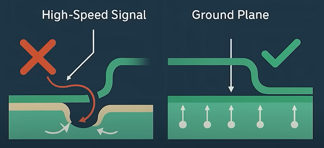
Whether using microstrip or stripline, USB differential pairs require a complete (not broken) reference plane to provide the shortest return path. This is especially critical for USB 3.0 and above.
USB Design in KiCad
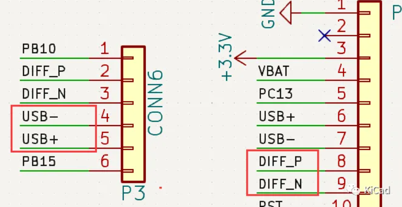
When designing the schematic, it is essential to define the differential pair signals using the _P/_N or +/- suffix:
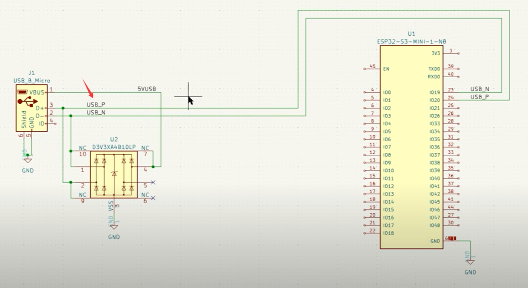
Since USB interfaces are exposed to the outside of the system and are frequently plugged and unplugged, it is strongly recommended to add ESD protection chips to prevent damage to relatively expensive main chips (such as the main CPU, USB controller, power management IC, etc.) due to static electricity or other accidental situations. Any interface directly connected to the outside must consider protection against electrostatic discharge (ESD) and electromagnetic interference (EMI). ESD protection devices (such as TVS diodes) and common mode chokes should be reasonably laid out on the data lines and power lines near the USB connector. ESD devices can instantaneously clamp harmful static voltages, protecting subsequent circuits; while common mode chokes can effectively suppress common mode noise on the differential lines, further enhancing the signal’s immunity to interference. The layout principle for these protective devices is to place them as close to the connector as possible, absorbing or filtering harmful energy before it enters deep into the main board.
When performing PCB layout, the following points should be noted:
1. If the differential pair is on the top or bottom layer (microstrip), there must be a complete reference ground plane below, and signal crossing over plane breaks is not allowed.
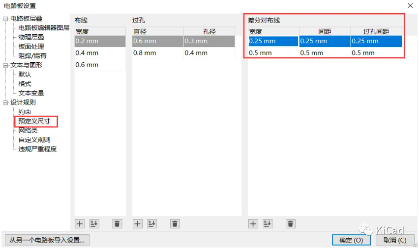
 2. Use custom DRC rules to limit the trace width, spacing, and maximum uncoupled length of the differential pair.
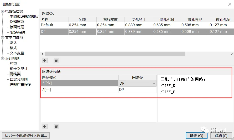
 We can also define a network class for a differential pair using wildcards or regular expressions:
 Then use “custom rules” to define special rules for the DP differential pair network class. For example, the following image defines the spacing for the differential pair: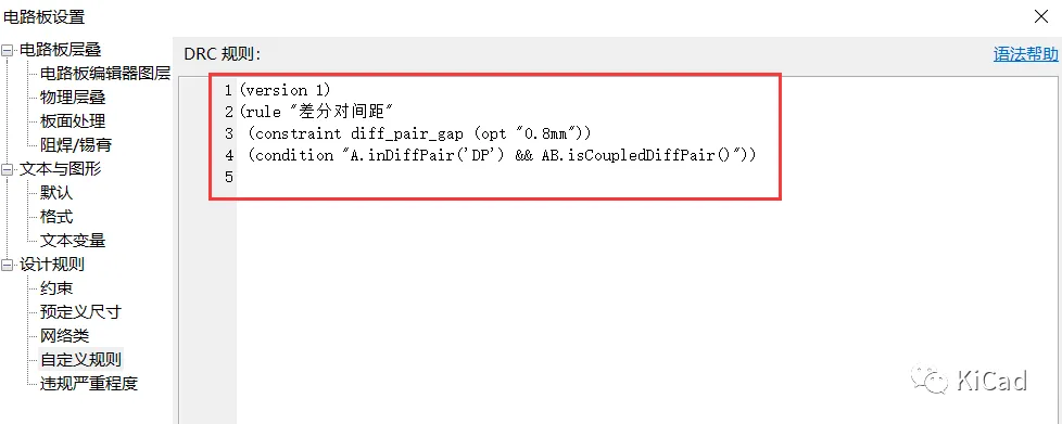
Additional Requirements for USB 3.0
For USB 3.0, these principles need to be executed even more rigorously, with attention to the following special and critical requirements:
1. Strict Impedance Control: Not Just D+/D-
USB 3.0 introduces a new SuperSpeed differential pair: one pair for transmission (SSTX+/SSTX-), and one pair for reception (SSRX+/SSRX-). These two pairs are independent of the original USB 2.0 D+/D- lines.
-
Target Impedance: All SuperSpeed differential pairs (SSTX and SSRX) must strictly control 90 ohms ±7% differential impedance. Compared to USB 2.0’s 90 ohms ±15%, this tolerance requirement is twice as strict. This means you need to accurately determine the trace width, spacing, and reference plane distance through PCB stack-up design and impedance calculation tools.
-
D+/D- Lines: At the same time, the D+/D- lines on the board must still maintain a 90-ohm differential impedance to be compatible with USB 2.0 mode.
2. Extreme Length Matching for Differential Pairs
At a rate of 5 Gbps, even slight differences in signal propagation time can lead to data sampling errors.
-
Length Matching: The length difference between SSTX+ and SSTX-, as well as between SSRX+ and SSRX-, must be controlled within a very small range. The industry typically recommendsnot exceeding 5 mil (0.127 mm). This usually requires precise compensation by adding serpentine traces on shorter traces.
-
Note that the SSTX differential pair and SSRX differential pair donot need to be length matched.
3. Clear Isolation and Spacing Requirements
High-speed signals are very susceptible to external noise interference and can easily cause interference to the outside.
-
Away from Noise Sources: SuperSpeed differential pairs should be kept away from oscillators, clock lines, switch-mode power supplies (SMPS), and other periodic signal lines. A common rule of thumb is the “3W principle”, which states that the spacing between high-speed lines and other signal lines should be at least three times the line width.
-
Differential Pair Spacing: To prevent crosstalk, there should be sufficient distance between SSTX and SSRX differential pairs, as well as between them and D+/D- differential pairs, with a recommended spacing of at least 20 mil (0.5 mm).
4. Complete Reference Plane and Shortest Return Path
This is the foundation of all high-speed designs, but it is especially important in USB 3.0.
-
Continuous Reference Plane: The trace below the SuperSpeed differential pair must have acomplete and continuous ground plane (GND Plane). Crossing over ground plane split areas is absolutely not allowed. The return path of the signal will follow the ground plane directly beneath the trace back to the source, and any interruption will greatly disrupt impedance continuity, creating an antenna effect.
-
Multilayer Boards are Standard: It is strongly recommended to useat least a four-layer board (signal layer-ground layer-power layer-signal layer). This provides an ideal, low-impedance reference plane for high-speed signals.
5. Minimize and Optimize Via Usage
Vias are “sinkholes” on high-speed signal paths.
-
Avoid Whenever Possible: Vias should be avoided on the path of SuperSpeed differential pairs whenever possible. Vias introduce parasitic capacitance and inductance, which are serious points of impedance discontinuity.
-
When Necessary: If unavoidable, vias must beused in pairs and symmetrically, and “ground vias” (stitching vias) should be placed next to the vias to ensure continuity of the signal return path.
Key Differences in Routing Between USB 2.0 and USB 3.0
| Design Parameter | USB 2.0 | USB 3.0 | Special Requirements |
| Differential Pair Count | 1 pair (D+/D-) | 3 pairs (D+/D-, SSTX, SSRX) | Two new independent high-speed differential lines added |
| Differential Impedance | 90 Ω ± 15% | 90 Ω ± 7% | Tighter tolerance requirements, more precise control |
| Length Matching | < 50 mil (1.27mm) | < 5 mil (0.127mm) | Extremely strict requirements, key to design success |
| Trace Length | Recommended < 5 meters (depends on cable) | Recommended PCB trace < 6 inches (15 cm) | High-frequency attenuation is severe, PCB traces must be as short as possible |
| PCB Layer Count Recommendation | 2-layer board is acceptable | Strongly recommend 4 layers or more | Requires dedicated ground and power layers |
| Via Usage | Minimize | Avoid as much as possible, must optimize | Vias have a much greater impact on 5Gbps signals than on 480Mbps |
In summary, the layout and routing of USB 3.0 is no longer a simple matter of “just connecting the lines”; it requires the application of signal integrity knowledge from the RF and microwave fields. Every corner, every via, and every millimeter of length difference can become a decisive factor affecting final performance.
Conclusion
Successful USB PCB routing does not rely on some mysterious intuition, but is built on rigorous engineering practices grounded in a deep understanding of signal integrity, impedance control, and electromagnetic compatibility. From safeguarding the core differential pairs, providing them with a complete reference plane, ensuring clean power, and building a solid protective barrier, every step is crucial. By following these best practices, your design will no longer be left to chance, and every connection will guarantee stability and efficiency.
If you want to receive KiCad content updates first, please click the card below, follow, and set it as a star.
Common Collection Summary:
-
Learn KiCad with Dr. Peter
- KiCad 8 Exploration Collection
- KiCad Usage Experience Sharing
- KiCad Design Projects (Made with KiCad)
- Common Problems and Solutions
- KiCad Development Notes
- Plugin Applications
- Release Records