 The increasing number of high-frequency signal designs is closely linked to the steadily improving performance of electronic systems. As system performance improves, PCB designers face growing challenges: smaller grain sizes, denser circuit board layouts, and lower power consumption requirements for chips. Technological advancements are always accompanied by a series of issues. With the enhancement of system performance and the adoption of high-speed designs, certain problems must be addressed within the design environment.Below, we summarize the challenges faced:Signal QualityIC manufacturers tend to favor lower core voltages and higher operating frequencies, leading to sharply rising edge rates. Edge rates in unterminated designs can cause reflections and signal quality issues.CrosstalkIn high-speed signal design, dense routing often leads to crosstalk—an electromagnetic coupling phenomenon between traces on the PCB. Crosstalk can occur from edge coupling on the same layer or wide coupling on adjacent layers. Coupling is three-dimensional. Compared to side-by-side routing paths, parallel paths and wide traces can cause more crosstalk.
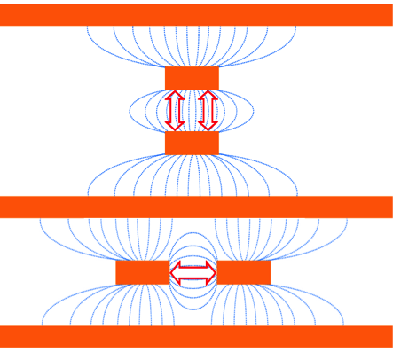 Wide coupling (top) compared to edge coupling (bottom)RadiationIn traditional designs, fast edge rates can produce ringing on unterminated transmission lines, even when using the same frequency and trace length as before. This fundamentally leads to higher radiation, far exceeding the FCC/CISPR Class B limits for unterminated transmission lines.
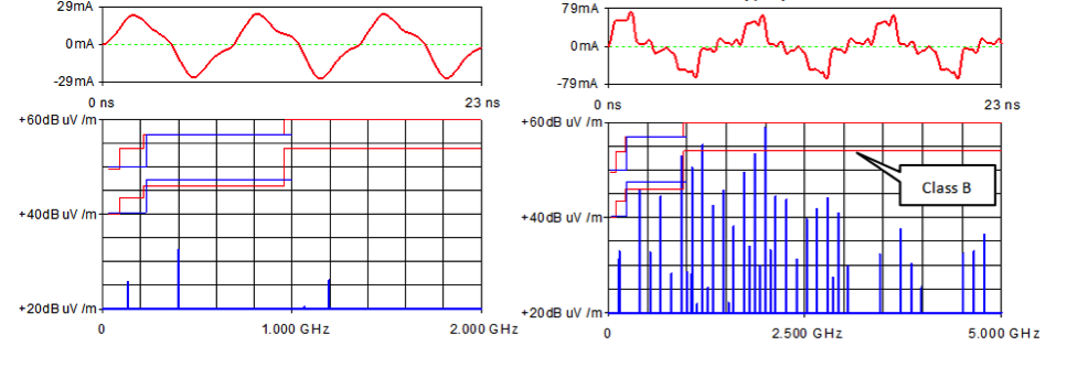 10 ns (left) and 1 ns (right) edge rate radiationDesign SolutionsSignal and power integrity issues can intermittently arise, making them difficult to diagnose. Therefore, the best approach is to identify and eliminate the root causes during the design process rather than attempting to resolve them in later stages, which can delay production. Layer planning tools can make it easier to implement solutions for signal integrity issues in your design.PCB Layer PlanningOne of the top priorities in high-speed design is PCB layer planning. The substrate is the most critical component in assembly, and its specifications must be carefully planned to avoid discontinuous impedance, signal coupling, and excessive electromagnetic radiation. When reviewing the PCB layers for your next design, keep the following tips and recommendations in mind:– All signal layers should be adjacent and tightly coupled to a continuous reference plane, which can create a clear return path to eliminate wide edge crosstalk.Each signal layer’s substrate should be adjacent to the reference plane– Good plane capacitance is necessary to reduce AC impedance at high frequencies. Tightly coupled inner layer planes can significantly reduce AC impedance on the top layer, greatly minimizing electromagnetic radiation.– Reducing dielectric height can greatly decrease crosstalk without impacting the usable space on the PCB.– The substrate should accommodate a range of different technologies. For example: 50/100 ohm digital, 40/80 ohm DDR4, 90 ohm USB.Routing and WorkflowAfter carefully planning the layers, the next step is to focus on PCB routing. Based on well-defined design rules and work areas, you can efficiently and successfully route the PCB. The following tips can help make your routing easier and avoid unnecessary crosstalk, radiation, and signal quality issues:– Simplify views to clearly see split planes and current loops. To do this, first determine which copper plane (ground or power) serves as the reference plane for each signal layer, then open the signal layer and inner layer planes simultaneously. This will help you more easily visualize the routing across the split plane.
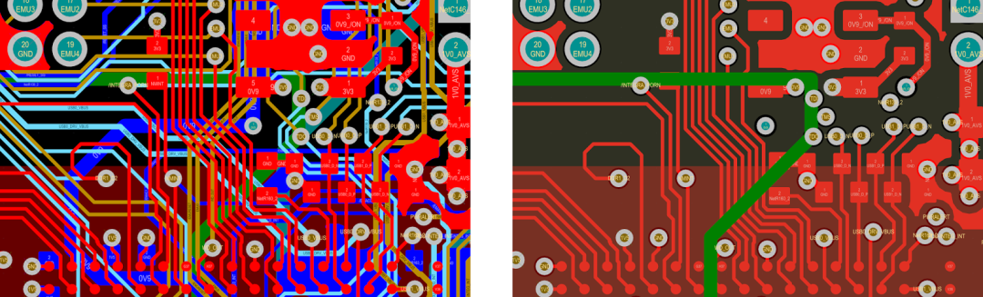 Multiple signal layers (left), top layer and adjacent plane view (right)– If digital signals must cross a power reference plane, you can place one or two decoupling capacitors (100nF) close to the signal. This provides a current loop between the two power sources.– Avoid parallel routing and wide traces, as these can cause more crosstalk than side-by-side routing.– Unless using a synchronous bus, keep parallel intervals as short as possible to reduce crosstalk. Leave space for signal groups so that the address and data spacing is three times the trace width.– Be cautious when using combined microstrip layers on the top and bottom of the PCB. This can lead to crosstalk between traces on adjacent layers, jeopardizing signal integrity.– Route the longest delay of the signal group as the clock (or strobe) signal trace, ensuring that data is established before the clock reads it.– Routing embedded signals between planes helps minimize radiation and provides ESD protection.By Barrey Olney, Source: https://www.altium.com.cn/blog/how-to-avoid-common-signal-integrity-issues-in-your-designs-CNEND
Apply for a free development board

For submissions/promotion/collaboration/joining groups, please scan the QR code to add WeChat(Please note your intention, and if joining a group, specify city-name-industry position information)
END
Popular Recommendations:
Which comes first, the fuse or the TVS? Two groups of engineers are arguing!
Profitable products easily cracked this way
Disassembling a telecom set-top box, a textbook case of hardware design cost reduction!
Why is there often a demand for MOSFETs to turn off quickly, but not for them to turn on quickly?
Why do MOSFETs need driver circuits?
Battery sampling circuit anomalies? Almost had to run away…
Guess what! High power ripple, can changing the inductor help?
I am the best lighting master in the electronics circle, the brightest guy!
Hardware engineers who don’t understand pricing, don’t take private jobs! Otherwise…