Abstract
“A 3D chip the size of a fingernail contains hundreds of billions of transistors, but the number of ‘pins’ to test it may be fewer than that of an old SIM card!” This statement left a deep impression on me during a recent conversation with semiconductor engineers.
As chip design transitions from 2D to 2.5D/3D ICs, the testing industry is facing a “sweet trouble.” The transistor density doubles every 18 months, leading to an explosive increase in the number of test vectors; traditional serial testing resembles a single-lane queue, while the ATE’s pin resources are as congested as a subway entrance during rush hour. Even more troubling is that prolonged testing times directly increase costs,chip manufacturers must balance performance with the “testing budget”.
Recently, Siemens Digital Industries Software has unveiled a trump card,Tessent IJTAG Pro, claiming to use “parallel magic” to solve this dilemma. Is this just a marketing gimmick, or can it truly change the game? Let’s break it down.
What Does Tessent IJTAG Pro Do?
First, let’s look at a set of real challenges:
-
Explosive Growth in Test Vector Quantity:In 3D stacked chips, a single die may contain dozens of IP modules, each requiring an independent test path.
-
Severe Limitation of ATE Resources:The number of test interface pins is limited, making it impossible to drive all scan chains simultaneously.
-
Longer Testing Time = Soaring Costs:According to SEMI data, advanced packaging testing costs account for over 30% of total manufacturing costs.
-
Inefficient Serial Transmission:Traditional IJTAG based on IEEE 1687 standard uses serial access, with data throughput as slow as “single-lane traffic jams.”
Siemens is not making minor adjustments this time; they are fundamentally restructuring the architecture. The core breakthroughs are threefold:
-
Serial → Parallel: A Qualitative Leap in Testing Speed
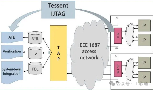
Traditional IJTAG resembles a narrow alley where data can only enter and exit one at a time. In contrast, Tessent IJTAG Pro leverages the wide bus architecture of the Tessent Scan Network (SSN) to transform this narrow alley into a “highway,”allowing multiple test data to be transmitted synchronously in parallel.
-
High Bandwidth Internal JTAG + Universal Data Flow
IJTAG Pro not only supports the standard IEEE 1687 but also introduces customized hardware read/write access capabilities, allowing engineers to configure dedicated data channels for specific IP modules. This means:whether it’s analog circuits, memory, or AI accelerator units, they can achieve optimal test paths.
-
Deep Collaboration with Tessent AnalogTest
Released earlier this year, Tessent AnalogTest specializes in analog/mixed-signal testing. After seamless integration with IJTAG Pro,the bandwidth for digital and analog testing is synchronized,truly achieving “one-stop testing for the entire chip.”
Not Just Fast, But Also “Flexible” and “Scalable”
Many readers may ask: Is this solution only suitable for large companies? Does it depend on specific processes?
The answer is no.
Siemens emphasizes:No matter if you are designing a single high-performance SoC or integrating multiple dies into a 2.5D/3D package, IJTAG Pro can dynamically allocate testing resources through the SSN architecture. In other words:
-
Small companies can use it to reduce ATE usage time and save costs;
-
Large companies can use it to support parallel verification of thousands of IP modules, accelerating mass production ramp-up.
This“on-demand scalability” capability is precisely what the current Chiplet ecosystem needs in terms of testing infrastructure. The value of Tessent IJTAG Pro lies inits embedded testability thinking from the early design phase and ensuring consistency throughout the process through standardized interfaces. This is not just an upgrade of tools, but alsothe practical implementation of design-manufacturing-testing integration.

In the past, testing was the “supporting role” in the manufacturing process; now, in an era where Moore’s Law is slowing down and Chiplets are on the rise,efficient testing capability has become a core variable in whether products can iterate quickly, control costs, and ensure yield.
The emergence of Siemens Tessent IJTAG Pro may not solve all DFT problems overnight, but it provides a clear path,using architectural innovation to combat complexity and leveraging parallel bandwidth to gain time windows.
