Introduction
JTAG is something that IC and embedded enthusiasts must have used, but for those who don’t understand the internal workings of JTAG and its implementation, this article is worth a read.
For those who have previously learned about coresight, you are aware of ARM’s internal debugging, knowing that the entry point for debugging lies in the JTAG Port. But how much do you really know about the external JTAG Port? Is it really just a simple port?
If you’re unfamiliar with coresight, you can check out 【Follow the Predecessors to Learn About Coresight】 for more information.
Why is it important to understand this? Recently, while debugging JTAG, I had to use some scripts and was quite curious about these commands, so I decided to investigate how these commands work within JTAG. Without further ado, let’s get started.
[PS: Thanks to the excellent blogs of predecessors at the end of this article for reference, as well as outstanding open-source documentation]
1- Overview of JTAG
1- What is JTAG
-
• JTAG: Joint Test Action Group
-
• Boundary scan requires compliance with IEEE 1149.1 (JTAG) standards
-
• BSDL (Boundary-Scan Description Language)
-
• Boundary-Scan TEST: A testing method for devices compliant with IEEE 1149.1 standards, generating test vectors through BSDL files to test devices for open and short circuits
Boundary scan testing developed in the 1990s with the advent of large-scale integrated circuits. As the manufacturing process of printed circuit boards has evolved to smaller, thinner designs, traditional ICT testing is no longer sufficient to meet the testing requirements of such products. Due to the high number of pins on chips, small component sizes, and extremely high board density, probing tests are simply not feasible. A new testing technology emerged, defined by the Joint Test Action Group (JTAG) as boundary scan testing.
With the use of surface mount technology, the density of printed circuit boards (PCBs) has increased, making traditional bed-of-nails testing techniques impractical. Adding test points or additional test circuits to complex circuits for individual testing are merely improvements to traditional methods, offering limited effectiveness and poor generality.
To improve the testability of circuits and systems, Philips Electronics first proposed and collaborated with other electronic device manufacturers in Europe, North America, and Asia to form the Joint Test Action Group (JTAG) in 1985. In February 1990, JTAG collaborated with the IEEE standards committee to propose the IEEE 1149.1 standard for “Standard Test Access Port and Boundary Scan Architecture”. This standard requires the inclusion of boundary scan circuits in integrated circuits.
During board-level testing, a shift register chain can be formed under control of mode selection, allowing for scanning of all pins of the integrated circuit, checking for solder faults and connection faults on the printed circuit board by serially inputting test data into this register chain, greatly facilitating the debugging of system circuits. The promotion and application of the IEEE 1149.1 standard have led to significant changes in testing equipment and systems, and boundary scan testing technology is increasingly becoming the mainstream testing technology for ultra-large-scale integrated circuits.
2- Benefits of Using JTAG
-
• Shortens product time to market
-
• Reduces testing costs
-
• Improves product quality and reliability
-
• Lowers PCB costs
Conclusion
Boundary scan testing has two major advantages:
-
• One is the convenience of locating chip faults, allowing for quick and accurate testing of whether two chip pins are reliably connected, improving testing efficiency;
-
• The other is that chips with JTAG interfaces have some predefined functional modes built-in, allowing the chip to be set to a specific functional mode via the boundary scan channel, enhancing system control flexibility and facilitating system design.
2- Structure of Boundary Scan Devices
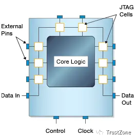
JTAG aims to solve the difficulties of testing circuits using traditional ICT methods.
Modern packaging technologies (such as BGA and chip-level packaging) limit and in some cases eliminate physical access to pins.
JTAG overcomes this problem by placing units (boundary scan units) between the device’s external connections and internal logic, as shown in the figure above. By configuring these units as shift registers, JTAG can monitor/control the values of these pins (and the networks connected to them) without direct physical access, greatly reducing the need for physical access to the board.
During normal operation, it is also possible to sample the data values transmitted between the chip and its pins, allowing real-time observation of the pin states.
Each unit in this register is located at the boundary of the device, between its core logic and the pins connected to the board—hence JTAG testing is also referred to as boundary scan.
For devices that must comply with JTAG standards, manufacturers must provide BSDL files (Boundary Scan Description Language), which describe how the device’s JTAG aspects work.
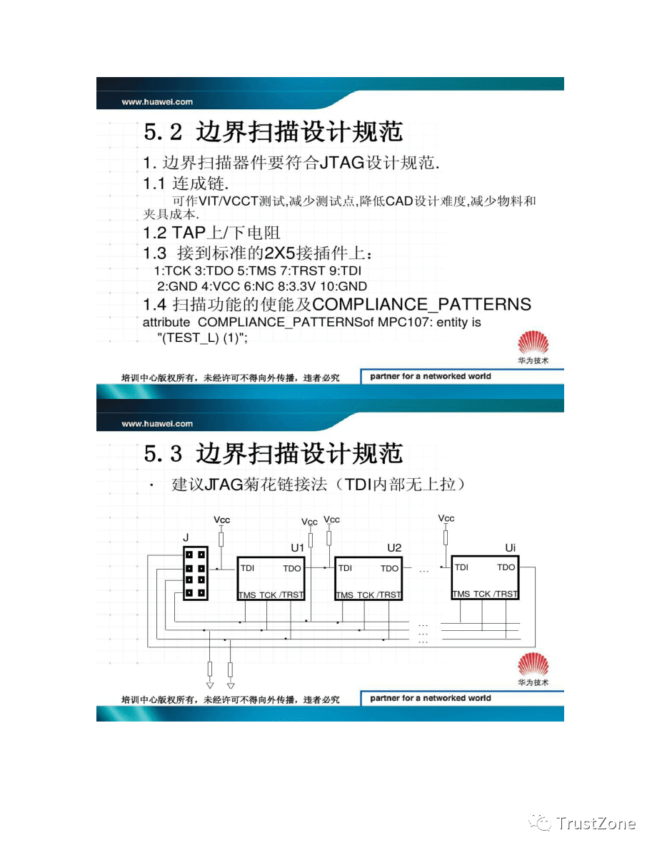
If a circuit contains multiple JTAG-compatible devices, these devices can be linked together to form a JTAG chain.
In a JTAG chain, the data output from the first device becomes the data input for the second device.
Control and clock signals are common for all devices in the chain, ensuring that the devices maintain the same state during testing.
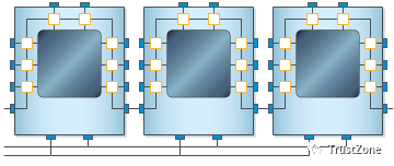
If you still don’t understand this link, no worries, continue watching this afternoon, it’s not a subsequent blocking point.
0- Boundary Scan
In JTAG debugging, boundary scan is a very important concept.
The basic idea of boundary scan technology is to add a shift register unit to the input/output pins near the chip. Since these shift register units are distributed around the boundaries of the chip, they are called boundary scan register cells.
When the chip is in debug mode, these boundary scan registers can isolate the chip from the peripheral inputs and outputs. Through these boundary scan register units, observation and control of the chip’s input and output signals can be achieved.
-
• For the chip’s input pins, signals (data) can be loaded into those pins through the connected boundary scan register units;
-
• For the chip’s output pins, signals can also be “captured” (CAPTURE) from those pins through the connected boundary scan registers.
In normal operation, these boundary scan registers are transparent to the chip, so normal operation is not affected. Thus, boundary scan registers provide a convenient way to observe and control the chips that need debugging.
Additionally, the boundary scan (shift) register units on the chip’s input/output pins can be interconnected to form a boundary scan chain around the chip. Generally, chips will provide several independent boundary scan chains to achieve complete testing functionality. The boundary scan chain can input and output serially, and through corresponding clock and control signals, it can conveniently observe and control the chips in debug mode.
Next question: How to manage and use these boundary scan chains?
Control of the boundary scan chain is mainly accomplished through the TAP (Test Access Port) Controller.
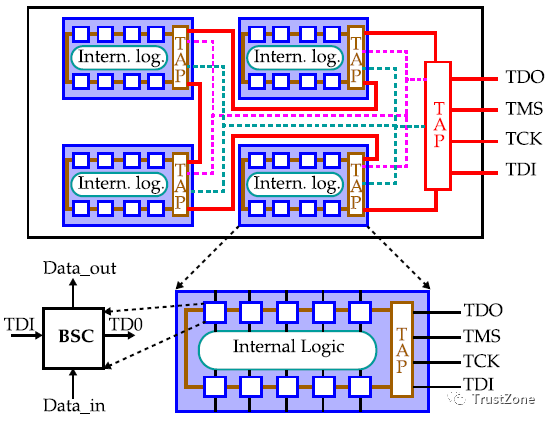
1- Hardware Structure of Boundary Scan
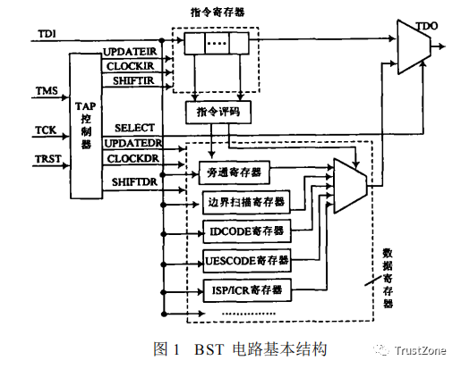
The core idea of BST is to add a group of shift registers between the chip pins and the internal logic of the chip, at each input and output pin of the component. In the PCB test mode, the register units, under the action of corresponding instructions, control the state of output pins and read the state of input pins, allowing users to test the interconnections on the PCB.
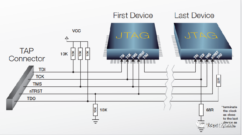
The BST circuit mainly includes
-
• Instruction Register (IR),
-
• Bypass Register (BR),
-
• Boundary Scan Register (BSR)
-
• Test Access Port (TAP) Controller.
The BST circuit generally uses a 4-wire test bus interface, as shown in Figure 1. If the test signal includes a reset signal (nTRST), a 5-wire test bus interface is used.
The five signals are:
-
• Test Data Input Bus (TDI), which inputs test data into the shift register (SR);
-
• Test Data Output Bus (TDO), which outputs test data from SR;
-
• Test Clock Bus (TCK);
-
• Test Mode Select Bus (TMS), which controls various testing processes, such as selecting registers, loading data, forming tests, outputting results, etc.;
-
• Reset Signal Bus (TRST), active low.
The IEEE Std 1149.1 test bus uses two clock edges of TCK,
-
• TMS and TDI are sampled on the rising edge of TCK,
-
• TDO changes on the falling edge of TCK.
2- TAP (Test Access Port)
In the previous section, we briefly introduced the boundary scan chain, and we also learned that general chips will provide several boundary scan chains to achieve complete testing functionality. Next, I will gradually introduce how to control and access the scan chain.
In the IEEE 1149.1 standard, registers are divided into two main categories:
-
• Data Register (DR)
-
• Instruction Register (IR)
The boundary scan chain is a very important type of data register.
-
• The boundary scan chain is used to observe and control the chip’s input and output.
-
• The instruction register is used to control the data registers.
For example, among all the boundary scan chains provided by the chip, one specific boundary scan chain is selected as the current target scan chain and access object. Now, let’s start with the TAP (Test Access Port).
2.1 Interface Signal Definitions
TAP is a universal port, through which all data registers (DR) and instruction registers (IR) provided by the chip can be accessed. Control of the entire TAP is accomplished through the TAP Controller. TAP includes a total of five signal interfaces: TCK, TMS, TDI, TDO, and TRST; where four are input signal interfaces and one is an output signal interface.
Generally, we see a JTAG interface on development boards, and the main signal interfaces of this JTAG interface are these five. Below, we will introduce each of the five interface signals and their functions.
-
• Test Clock Input (TCK): TCK provides an independent, basic clock signal for TAP operations. All TAP operations are driven by this clock signal. TCK is mandatory in the IEEE 1149.1 standard.
-
• Test Mode Selection Input (TMS): The TMS signal is used to control the state transitions of the TAP state machine. Through the TMS signal, TAP can be controlled to switch between different states. TMS is valid on the rising edge of TCK. TMS is mandatory in the IEEE 1149.1 standard.
-
• Test Data Input (TDI): TDI is the data input interface. All data to be input into a specific register is serially input through the TDI interface (driven by TCK). TDI is mandatory in the IEEE 1149.1 standard.
-
• Test Data Output (TDO): TDO is the data output interface. All data to be output from a specific register is serially output through the TDO interface (driven by TCK). TDO is mandatory in the IEEE 1149.1 standard.
-
• Test Reset Input (TRST): TRST can be used to reset (initialize) the TAP Controller. However, this signal interface is optional in the IEEE 1149.1 standard and is not mandatory. Because the TAP Controller can also be reset (initialized) through TMS.
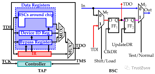
2.2 Instruction Register, Common Instructions, and Data Registers
In the IEEE 1149.1 standard, some instruction registers, common instructions, and related data registers are specified. For specific chips, chip manufacturers generally expand some private instructions and data registers based on the IEEE 1149.1 standard to facilitate testing and debugging during the development process. In this section, I will briefly introduce some commonly used instructions and their related registers as defined by IEEE 1149.1.
1- Instruction Register:
The instruction register allows specific instructions to be loaded into the instruction register, to select the tests to be executed or the test data registers to be accessed. Every chip that supports JTAG debugging must include an instruction register (IR).
2- BYPASS Instruction and Bypass Register:
The bypass register is a one-bit shift register that can be connected between TDI and TDO through the BYPASS instruction. When no testing is needed, the bypass register connects TDI and TDO, providing the shortest serial path between TDI and TDO. This allows test data to quickly pass through the current chip to other chips on the development board.
3- IDCODE Instruction and Device Identification Register:
The Device Identification register can include information about the manufacturer, part number, and version information of the device. By using the IDCODE instruction, the relevant information of the device can be determined through TAP. For example, ARM MULTI-ICE can automatically identify which chip is currently being debugged, which is actually done by accessing the Device Identification register through the IDCODE instruction.
4- INTEST Instruction and Boundary-Scan Register:
The Boundary-Scan register is what we referred to earlier as the boundary scan chain, and generally, a chip has multiple boundary scan chains. Through the boundary scan chain, connectivity testing between components can be performed. Of course, more importantly, it allows observation and control of the input and output of the test device to achieve testing of the internal logic of the device.
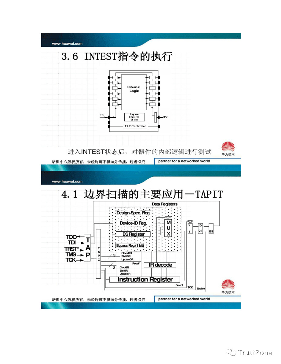
The INTEST instruction is a very important instruction defined in the IEEE 1149.1 standard: in conjunction with the boundary scan chain, this instruction allows internal testing of the system logic of devices on the development board. In ARM JTAG debugging, this is a frequently used test instruction.
As we mentioned earlier, registers are divided into two main categories: instruction registers and data registers. The bypass register, device identification register, and boundary-scan register (boundary scan chain) mentioned above all belong to data registers. In debugging, the boundary scan register (boundary scan chain) is the most important and frequently used.
In fact, the general process of accessing data registers (DR) through the TAP interface is:
-
• Select a data register (bypass, ID, Boundary-scan) to access through the instruction register (IR);
-
• Connect the selected data register between TDI and TDO;
-
• Driven by TCK, input the required data into the selected data register through TDI; simultaneously read the data from the selected data register through TDO.
SIR->TDI->TDO
3- TAP Controller
The JTAG interface adds four additional pins to each device:
The TAP interface must include: TCK, TMS, TDI, TDO
-
• TCK (Test Clock Input): Test clock input line
-
• TMS (Test Mode Selection): Test mode selection input line
-
• TDI (Test Data Input): Test data input line
-
• TDO (Test Data Output): Test data output line
-
• TRST (Test Reset Input): Test reset input line, (optional)
The TAP controller is the core controller of boundary scan testing.
Under the control of TCK and TMS, it can select to scan the instruction register or the data register, and control the various states of boundary scan testing.
TMS and TDI are sampled on the rising edge of TCK, while TDO changes on the falling edge of TCK.
-
• The TAP controller is a 16-state finite state machine
-
• The state of the TAP controller changes on the rising edge of TCK
-
• The TAP controller enters a logic reset state upon power-up
-
• Shift-IR state scans IR, TDO output is valid
-
• Shift-DR state scans DR, TDO output is valid
-
• In other states, TDO output is invalid
1- TAP Controller Pin Functions and Relationships 1
-
• When TCK is low, the test logic storage unit remains unchanged; TCK samples the TMS and TDI input values on the rising edge, and TDO output changes on the falling edge
-
• Test instructions and test data are input from the TDI input line into the instruction register (instruction register) and various data registers (various test data registers)
2- TAP Controller Pin Functions and Relationships 2
-
• TDO output is only valid during shifting (Shift-DR or Shift-IR)
-
• Test operations are controlled by the sequence of TMS input “1” and “0”
-
• TRST can be asynchronously reset
-
• When TMS remains high for five consecutive TCK clock cycles, the TAP controller (TAP controller) will automatically enter the test logic reset state (Test-Logic-Reset)
4- TAP State Machine
The state machine of the TAP controller is shown in Figure 2. On the right is the instruction register branch, and on the left is the data register branch.
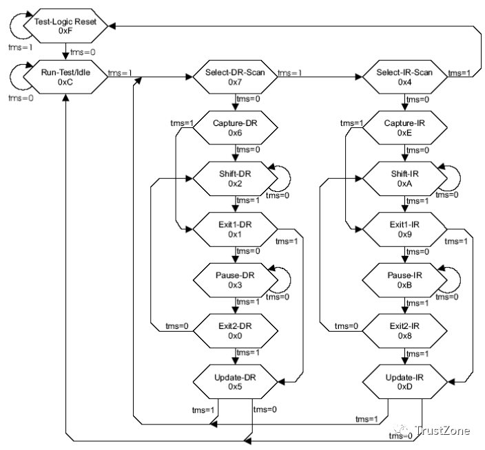
Among them, the TAP controller’s state machine has only six stable states:
-
• Test Logic Reset,
-
• Run Test Idle,
-
• Shift DR,
-
• Pause DR,
-
• Shift IR,
-
• Pause IR
Other states are not stable states but only transient states.
-
• When powered on or during normal operation of the IC, TMS must be held high for at least five TCK cycles to make TAP enter the test logic reset state. At this point, TAP issues a reset signal to ensure that all test logic does not affect the normal operation of the component.
-
• If boundary scan testing is required, it can exit the reset state under the control of TMS and TCK, entering the various states required for boundary scan testing.
-
• When testing is needed, under the control of TMS and TCK, the TAP controller jumps out of the TLR state (test logic reset), selecting either data register scanning (Shift DR Scan) or instruction register scanning (Shift IR Scan) to enter the various states shown in Figure 2. The functions of Shift DR Scan and Shift IR Scan modules are similar.
-
• The first step to enter each module is to capture data (Capture),
-
• For the data register, the data is parallel loaded into the corresponding serial data channel during the Capture DR state,
-
• For the instruction register, the instruction information is captured into the instruction register during the Capture IR state.
-
• The TAP controller transitions from the capture state to the shift (Shift) or exit 1 (Exit1) state. Typically, the Shift state follows the Capture state, with data shifting in the register.
-
• After the Shift state, the TAP controller transitions from Exit1 to the Update state or Pause state.
-
• In the Pause state, data shifting temporarily halts, allowing for reloading test vectors into the data register or instruction register.
-
• Exiting the Pause state can lead back into the Shift state or, through the Update state, return to the Run Test Idle state. In the Update state, the data scanned into the channel is output.
This state machine may seem complex, but once understood, it is actually very straightforward and simple. Observing the above figure, we can see that aside from the Test-Logic Reset and Test-Run/Idle states, the other states have some similarities. For example, Select-DR-Scan corresponds to Select-IR-Scan, Capture-DR corresponds to Capture-IR, Shift-DR corresponds to Shift-IR, and so on. In these corresponding states, DR represents Data Register, and IR represents Instruction Register. Do you remember what we discussed earlier? Registers are divided into two main categories: data registers and instruction registers. In fact, the states marked with DR are used to access data registers, while those marked with IR are used to access instruction registers.
Let’s take a more intuitive example. Now suppose the TAP Controller is currently in the Run-Test/Idle state, and a new instruction has been successfully written into the instruction register, selecting a boundary scan chain of length 6.
Now let’s see how to access this boundary scan chain. The figure below shows the test chip and the boundary scan chain of length 6 selected by the current instruction. From the figure, it can be seen that the currently selected boundary scan chain consists of six boundary scan shift register units, connected between TDI and TDO.
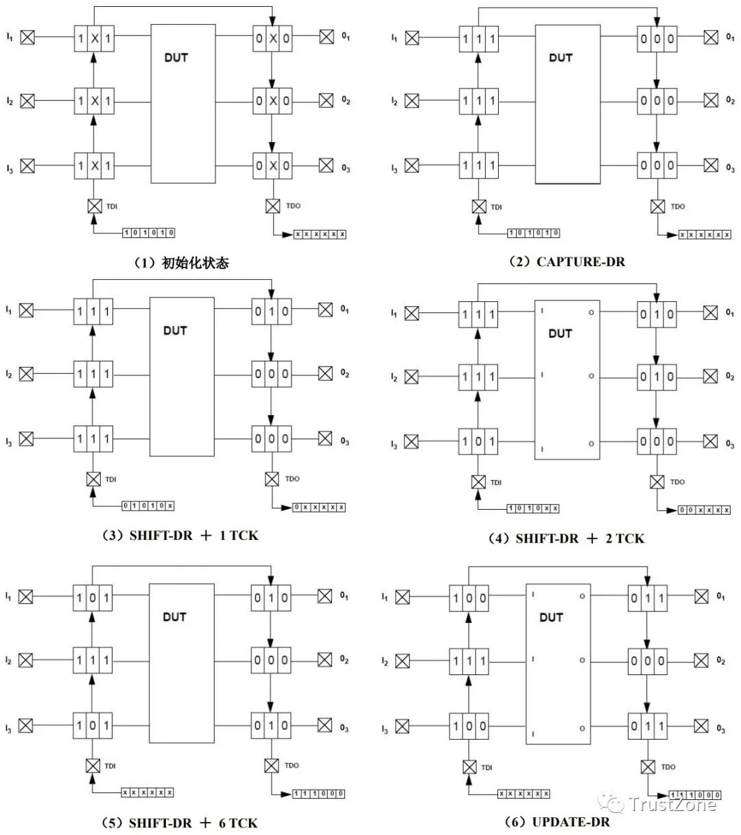
The TCK clock signal is connected to each boundary scan shift register unit. Each clock cycle can drive the data of the boundary scan chain to move one position from TDI to TDO, thus new data can be input one bit through TDI, and the data in the boundary scan chain can be output one bit through TDO. After six clock cycles, the data in the boundary scan chain can be fully updated, and the six bits of data captured in the boundary scan chain can be output entirely through TDO.
-
• The figure (1) shows the initial state of the chip and the boundary scan chain. In the testing state, the chip’s external inputs and outputs are isolated, and the chip’s inputs and outputs can be observed and controlled through the corresponding boundary scan chain.
-
• In figure (1), the data in each shift register unit of the scan chain is uncertain, so it is represented as X in the figure, resulting in a data sequence of XXXX.
-
• The data sequence to be input from TDI to the test chip is: 101010. Simultaneously, the corresponding states on the chip pins will be obtained from TDO.
-
• Now the TAP Controller transitions from the Run-Test/Idle state through the Select-DR-Scan state into the Capture-DR state. In the Capture-DR state, under the drive of one TCK clock, the signal states on the chip pins are all captured into the corresponding boundary scan shift register units, as shown in figure (2).
-
• From figure (2), we can see that after entering the Capture-DR state, after one TCK clock cycle, the data sequence in the scan chain changes to: 111000.
-
• After the data capture is complete, it transitions from the Capture-DR state to the Shift-DR state.
-
• In the Shift-DR state, we will input the new data sequence (101010) into the boundary scan chain through TDI over six TCK clock cycles;
-
• At the same time, the captured data sequence (111000) in the boundary scan chain will be output through TDO.
-
• After entering the Shift-DR state, with each TCK clock drive, one bit of data will be output from TDO; at the same time, one new data bit will be received from TDI.
-
• Figure (3) shows the changes in the scan chain after one TCK clock cycle in the Shift-DR state. Figure (4) shows the changes in the scan chain after two TCK clock cycles in the Shift-DR state. At this point, the scan chain has serially received two new data bits from TDI and also output two data bits from TDO. Under the drive of the TCK clock, this process continues. Figure (5) shows the situation of the scan chain after six TCK clock cycles.
-
• From figure (5), we can see that the boundary scan chain now contains the new data sequence: 101010. On the TDO side, after six TCK clock drives, the data sequence captured in the Capture-DR state is also received as 111000.
-
• Up to this point, although the scan chain contains the new data sequence: 101010, the state on the test chip’s pins remains as: 111000. The next step is to update the state of the corresponding pins on the test chip. To realize the update,
-
The TAP Controller transitions from the Shift-DR state through the Exit1-DR state into the Update-DR state. In the Update-DR state, after one cycle of TCK clock drive, the new data sequence in the boundary scan chain will be loaded onto the corresponding pins of the test chip, as shown in figure (6).
-
• From figure (6), it can be seen that the state of the test chip has been updated, and the state sequence on the corresponding pins has changed from 111000 to 101010. Finally, it transitions from the Update-DR state back to the Run-Test/Idle state, completing access to the selected boundary scan chain.
Regarding the Pause-DR/Pause-IR states
These two states are pause states. For example, if we want to read the corresponding pin states from a 48-length scan chain through a 32-bit bus, we need to read twice to get the corresponding 48-bit scan chain state. First, we read the high 32 bits during 32 TCK clock cycles, then enter the Pause-DR state waiting for the bus read response. After the response is complete, we transition back to the Shift-DR state to read the low 16-bit data.
5- BST Register Units
The boundary scan data register should include at least three types: Boundary Scan Register, Device Identification Register, and Bypass Register.
1- Boundary Scan Register
(1) The boundary scan register constitutes the boundary scan path, with each unit consisting of memory, sender/receiver, and buffer. The boundary scan units are placed near the input/output terminals of the integrated circuit and are connected end-to-end to form a shift register chain, with the start connected to TDI and the end connected to TDO. Under the action of the test clock TCK, the data added from TDI can move within the shift register chain for scanning.
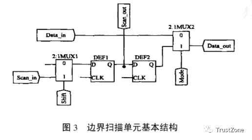
The basic structure of the boundary scan unit (BSC) is shown in the figure above. Its main function is to load test vectors and capture test responses.
D flip-flop, which changes its output based on the state of D under the action of a clock signal. DFF is edge-triggered, a data-triggered flip-flop (Data Flip-Flop) is a type of flip-flop that stores a single bit of data, commonly used in digital circuits, computer hardware, and embedded systems.MUX2 is controlled by the Mode signal,
-
• When the Mode signal is 0, the unit’s data output can be connected to the data input;
-
• When it is 1, the data output is the output signal of DFF2, independent of the data input signal.
The Shift signal controls MUX1,
-
• When it is 0, DFF1 samples the signal from the data input;
-
• When it is 1, shifting occurs.
The operation of BSC proceeds in the following four steps:
-
• MUX1 in Shift DR mode, new test vectors are shifted in;
-
• MUX2 in Update DR mode, loads test vectors to the unit’s data output;
-
• MUX1 in Capture DR mode, captures the response from the unit’s parallel input;
-
• MUX1 in Shift DR mode, shifts out the response.
2- Device Identification Register (ID)
The device identification register (ID) is 32 bits,
-
• Bits 31-28 are the version number,
-
• Bits 27-12 are the device serial number,
-
• Bits 11-1 are the manufacturer identification,
-
• Bit 0 is 1.
With it, the manufacturer of the components on the board can be identified, and it can also be used to test whether the correct device is installed in the correct position on the PCB. The device identification register and boundary scan register can use the same boundary scan unit.
3- Bypass Register (BR)
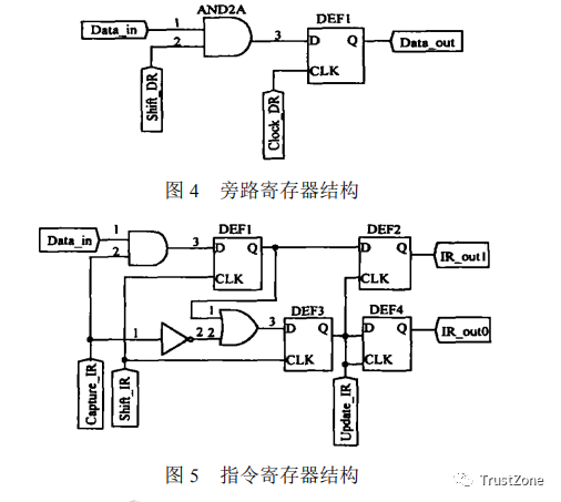
The bypass register (BR) is only 1 bit, providing the shortest path between TDI and TDO, to bypass the data of the data registers that do not participate in serial scanning, reducing unnecessary scanning time. The structure of the bypass register is shown in the figure below. In Shift DR mode, data flows directly from Data in to Data out, bypassing any boundary scan registers.
6- Instruction Register
The instruction register consists of a serial shift level and a parallel latch level, used for instruction decoding. The structure of a two-bit instruction register is shown in the figure above.
The number of bits is determined by the number of selected instructions, and there are many commonly used instructions. DFF1 and DFF2 perform two-bit instruction decoding under the control of Capture IR and Shift IR, loading instruction data into the instruction output during the Update IR mode, with the high bit in IR out1 and the low bit in IR out2.
The IEEE 1149.1 standard defines a large number of instructions, some of which are mandatory, some optional, and it also allows the definition of more specific design instructions to extend the functionality of the test logic.
In addition to the above data registers, user-defined data registers can also be included.
7- JTAG Instructions
1- JTAG Instructions
Mandatory Public Instructions
-
• BYPASS, SAMPLE/PRELOAD, EXTEST
-
• If there is a Device Identification Register, IDCODE must be provided; if it is a programmable IC, USERCODE must also be provided. Optional Public Instructions
-
• INTEST, RUNBIST IC manufacturers can customize Public or Private Instructions, and the information of Public Instructions must be disclosed.
2- JTAG Circuit Instruction Codes
-
• BYPASS: All 1s, IC manufacturers can reassign other binary codes
-
• EXTEST: All 0s, IC manufacturers can reassign other binary codes
SAMPLE/PRELOAD, INTEST, RUNTEST, IDCODE, USERCODE: IC manufacturers assign their own binary codes.
Unassigned binary codes indicate BYPASS.
3- Brief Introduction to BSDL
The BSDL file instructions for the FPGA device EP1C12F256 are:
-
• “BYPASS (1111111111), ” &
-
• “EXTEST (0000000000), ” &
-
• “SAMPLE (0000000101), ” &
-
• “IDCODE (0000000110), ” &
-
• “USERCODE (0000000111), ” &
-
• “CLAMP (0000001010), ” &
-
• “HIGHZ (0000001011);
4- Execution of BYPASS Instruction
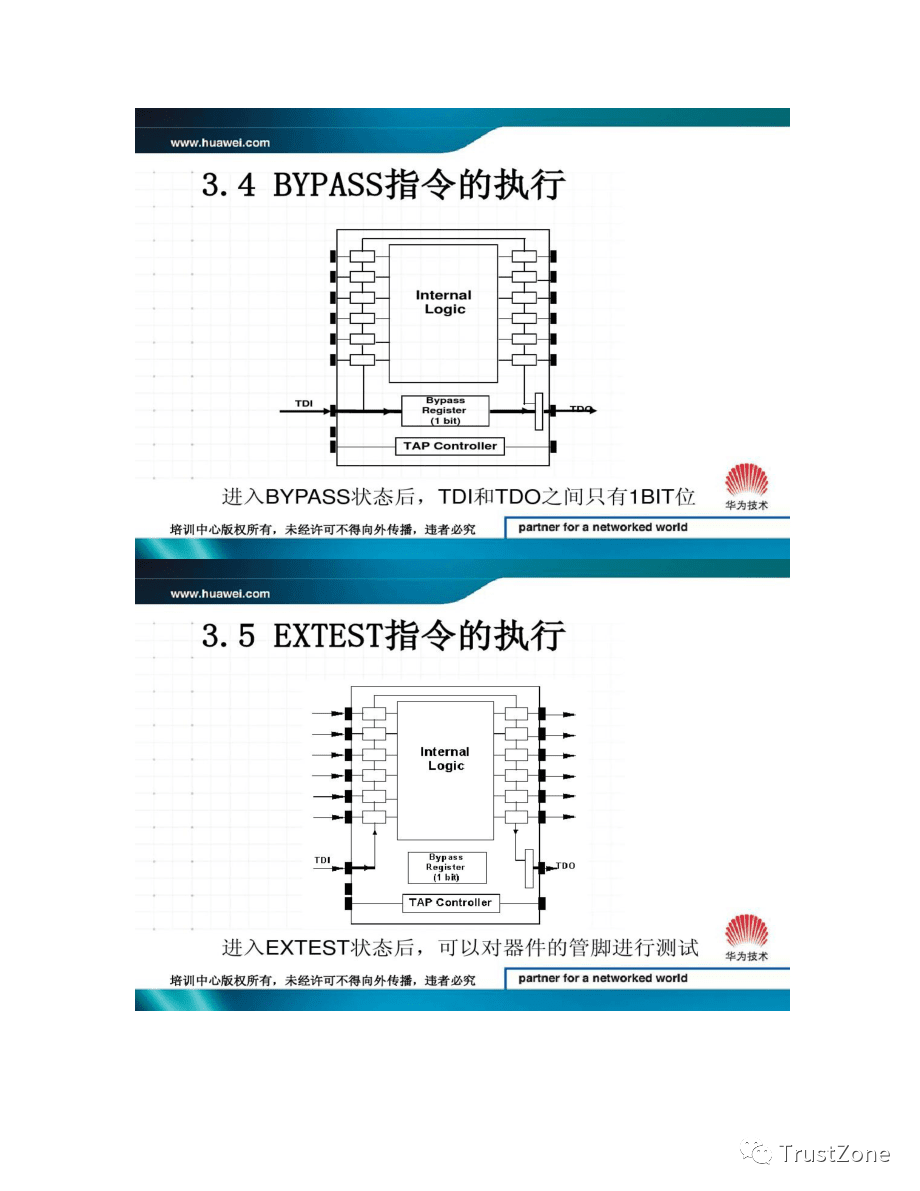
5- Execution of EXTEST Instruction
6- Execution of INTEST Instruction
3- Serial Vector Format File
Files created for testing programmable logic devices (PLD);
Contain descriptions of one or more test cases, such as combinational logic checks;
Used for debugging printed circuit boards (PCBs), integrated circuits (ICs), and embedded systems.
.SVF format complies with the Joint Test Action (JTAG) standard, also known as the standard test access port and boundary scan architecture.
SVF files are stored in ASCII text format and can be edited using a text editor.
.SVF automated test equipment (ATE) typically uses files that connect to the debug port in PLDs (programmable logic devices) to perform tests. PLDs without debug ports usually provide other mechanisms for stepwise logical testing.
Note: Serial vector format files can also be stored in binary format in .XSVF files.
4- Boundary Scan Testing Methods
Using boundary scan technology, a comprehensive understanding of internal faults in integrated circuit chips, interconnections on circuit boards, and mutual influences can be achieved, and the working modes can be selected by loading the corresponding instructions into the instruction register. Different tests are conducted under different working modes.
1- External Testing (EXTEST)
External testing tests the connection relationships between ICs and other components on the circuit board.
At this time, the boundary scan register isolates the internal logic of the IC from other components on the tested board.
Under the EXTEST instruction, a known value is assigned to each IO terminal to test the connections between various integrated circuit chips on the circuit board and the faults of board-level interconnections, including open circuit faults and short circuit faults.
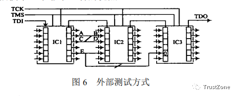
In figure 6, the three chips are controlled by the same TCK and TMS bus, with the TDO outputs of each chip connected to the TDI inputs of the next device, forming a shift register chain. The test vector is input from the TDI of IC1, through the boundary scan path to each chip’s output pin register, while the input pin registers receive the response vectors.
In the figure, pin B of IC2 receives the signal from pin A of IC1’s register; under normal circumstances, the value of pin B should be 1. However, if a short circuit occurs between lines AB and CD, the value received by pin B’s register will become 0. Pin F of IC3’s register receives the signal from pin E of IC1’s register; under normal circumstances, the value of pin F should be 1, but if an open circuit occurs between lines EF, the value obtained from pin F will be 0.
The most frequent faults in circuit board testing are open and short circuit faults. Traditional point-to-point inspection methods are both cumbersome and time-consuming, while through the external testing method of boundary scan technology, comparing the serial signals output from the boundary scan register at the TDO end with the correct signals can effectively diagnose open and short circuit faults between circuit board leads and chip pins. This is a very significant advantage of boundary scan technology.
2- Internal Testing (IN TEST)
Internal testing tests the logical functions of the IC itself, that is, testing the internal faults of integrated circuit chips on the circuit board.
The test vector is input through TDI, and the test vector is applied to each chip’s input pin register through the boundary scan channel, and the response results stored in the output pin registers of each chip can be read out serially from the TDO. Based on the input vector and output response, testing analysis can be conducted on the internal working states of each chip on the circuit board. (The output should have an expected value or expected result and phenomenon)
3- Sample Testing Method (SAMPLE/PRELOAD)
The sample testing method is commonly used for real-time monitoring of a running system. Sampling/Preloading (SAMPLE/PRELOAD),
-
• Samples from the input during the capture phase,
-
• Preloads BSC during the update phase, preparing for external testing;
-
• Outputs the device identification (ID Code): selects the bypass register, allowing data to shift quickly between ASICs.
4- Main Applications of Boundary Scan Chains
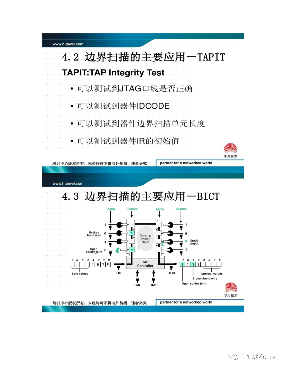
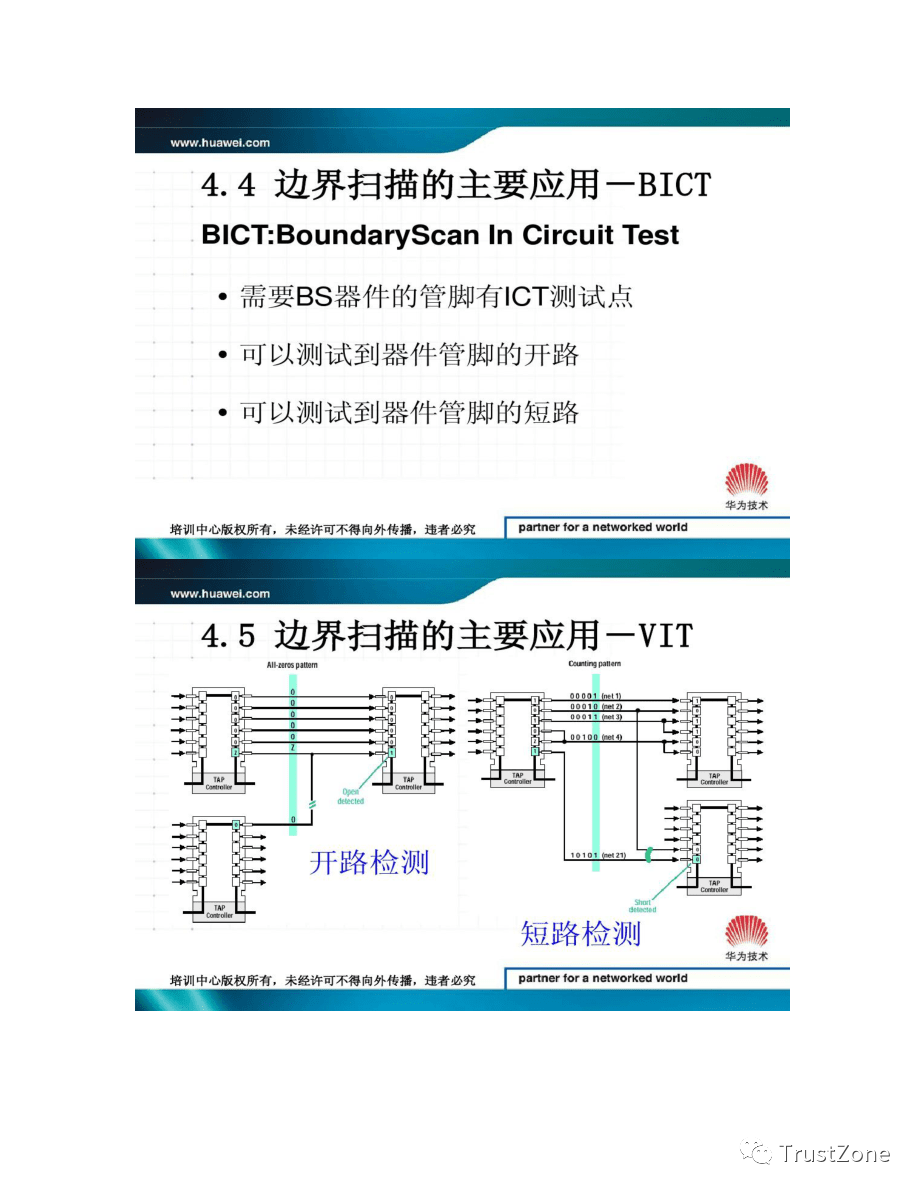
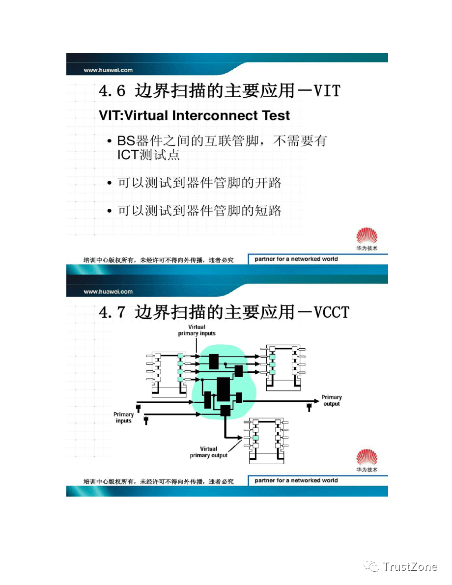
1- TAPIT
2- BICT
3- VIT
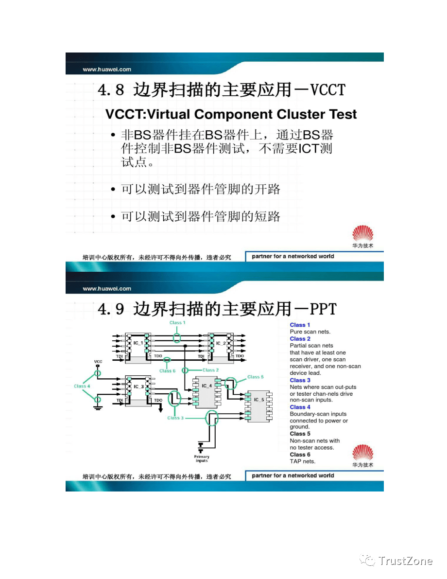
4- VCCT
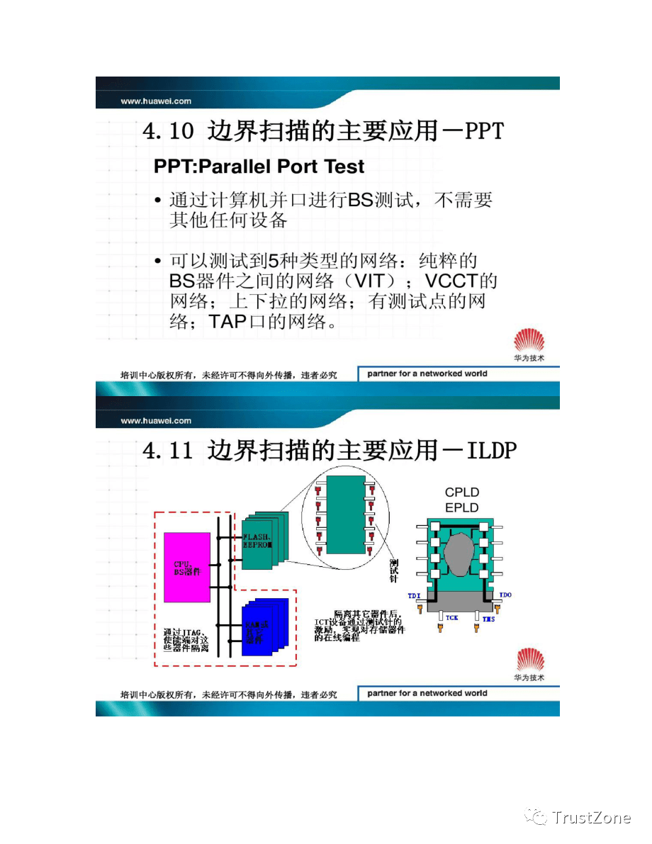
5- PPT
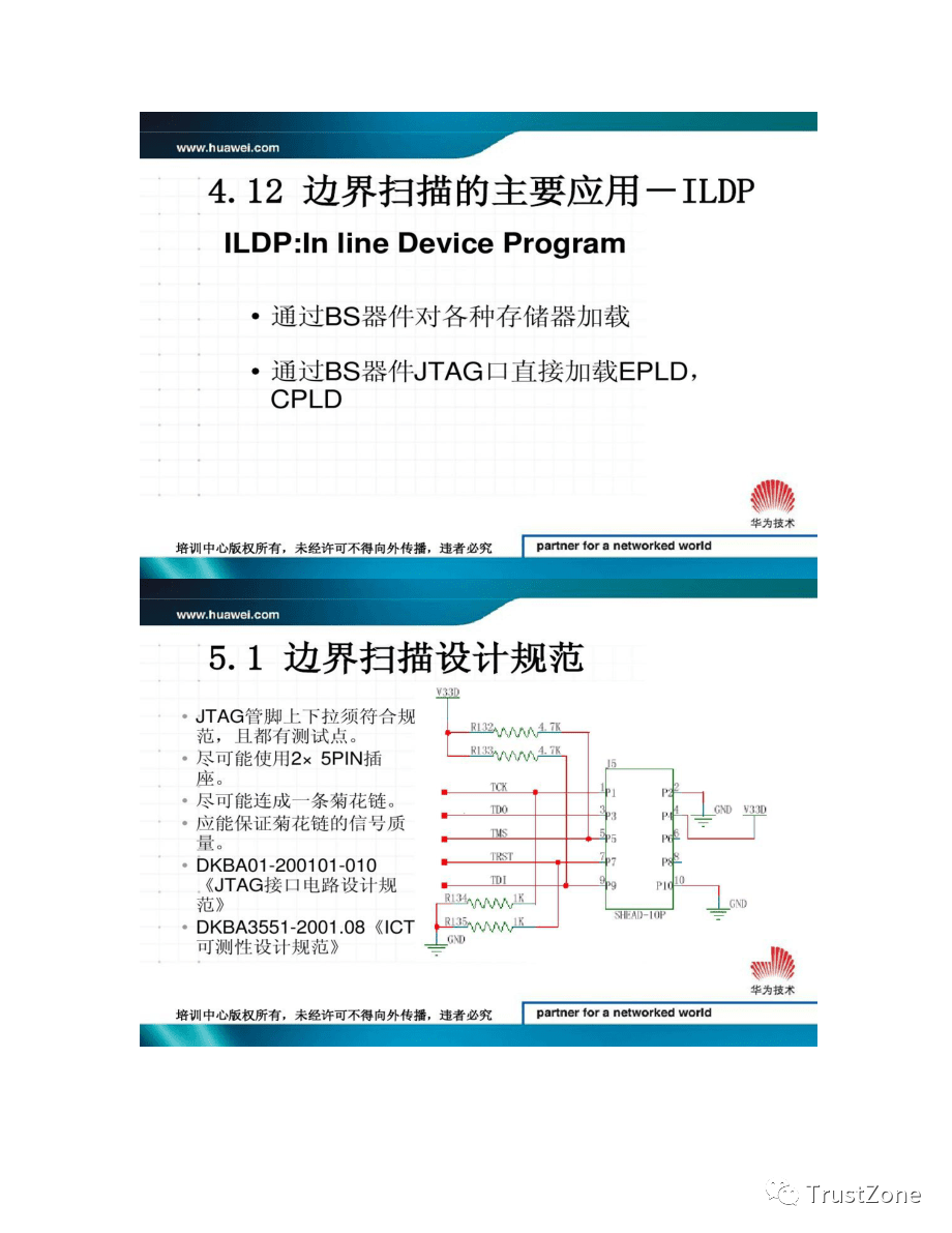
6- ILDP
5- JTAG Hardware Design
6- Conclusion
Additionally, there are various testing instructions, their existence and continuous expansion allow the application of boundary scan technology to be extended and enhanced, enabling more effective integrated circuit testing.
Boundary scan technology is a new testing technology that, while it can test the states of the input/output pins of integrated circuit chips, can also test the internal workings of chips and faults at the lead level. However, boundary scan technology is still under continuous development.
Its application is based on integrated circuit chips designed with boundary scan circuits. Testing of devices installed on circuit boards without boundary scan circuits is beyond the capabilities of boundary scan. In the future, it will not be possible to design boundary scan circuits into all digital integrated circuit chips, so it cannot completely replace other testing methods. The prominent advantage of this method is its testability, allowing faults in circuits or connections to be detected merely by running computer programs, making it particularly suitable for scenarios with high reliability requirements and short fault isolation times, especially in the built-in testing and maintenance of weapon systems.
References to excellent articles by predecessors:
-
• 【Analysis of the Principles of Boundary Scan Testing Technology】
-
• 【Working Principles of JTAG】
-
• 【Principles of TAG Boundary Scan Testing Technology】
Reference documents:
-
• http://fiona.dmcs.pl/~rkielbik/nid/IEEE_1149_JTAG_and_Boundary_Scan_Tutorial.pdf
-
• https://www.corelis.com/educationdownload/JTAG-Tutorial.pdf
-
• http://fiona.dmcs.pl/~cmaj/JTAG/JTAG_IEEE-Std-1149.1-2001.pdf