1. Common Terminology in FPGA
ECC (Error Correction Code):Error Correction Code
FIFO (First In First Out):First In First Out
IOB:Input Output Buffer
LUT (Look-up Table):Look-up Table
DSP (Digital Signal Processor):Digital Signal Processing, the DSP unit circuit includes basic logic units such as input, output, computation, and carry.
PLB (Programmable Logic Block):Programmable Logic Block
CLB (Configurable Logic Block):Configurable Logic Block, which refers to circuits that implement various logic functions, is the basic logic unit of Xilinx.
MGT:Abbreviation for High-Speed Serial Transceiver Module, operating speeds can reach 6~28Gb/s
HP: High Performance, High performance/high-speed interface, commonly used in memory, generally the maximum bank voltage can only reach1.8V
HR: High Range, Wide Range I/O, can support up to 3.3V voltage
HD: High Density, low-speed I/O, with a maximum speed limit of 250M, and a maximum voltage support of 3.3V
BRAM (Block RAM):Embedded Block RAM
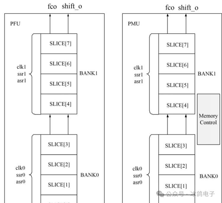
Slice:Slice, 2 or more slices constitute a CLB, also the basic unit of FPGA
CMT (Clock Management Tile):Clock Management Unit
DSP48x slices:Arithmetic processing module, capable of performing multiplication, addition, subtraction, and other logical calculations, can implementFinite Impulse Response (FIR) filtering and Fast Fourier Transform (FFT) calculations
AXI Interface:Advanced eXtensible Interface
2.Overview of FPGA
1.Introduction to FPGA Development
FPGA (Field Programmable Gate Array) is a type of programmable logic chip with general functionality, which can be programmed to perform specific logic processing functions. It has advantages such as high flexibility, short development cycles, and low costs for small batches. Therefore, it has a wide range of prospects and applications in traditional fields such as aerospace, communications, and industry, as well as in emerging areas like AI, 5G communications, industrial internet, autonomous driving, cloud computing, and edge computing.
The concept of FPGA can be traced back to the early 1980s. In 1984, Ross Freeman at Altera introduced the world’s first FPGA product, the Altera 2200;
In 1985, Xilinx was founded and launched the first FPGA based on Look-up Table (LUT) structure, the first commercial FPGA XC2064.
Currently, the mainstream market is mainly divided into four major camps: Xilinx (acquired by AMD), Altera (acquired by Intel), Lattice, and Microsemi, with the first two occupying over 90% of the market. See the previous article “Introduction to Foreign FPGA Manufacturers.”
Domestic development is relatively late, currently in the early development stage, with a smaller revenue scale and overall hardware performance indicators lagging behind Xilinx and Altera. However, in recent years, development has been rapid, with performance and scale catching up, and there is a subtle trend of surpassing.
There are mainly 8 domestic FPGA manufacturers: Unisoc, Guowei Electronics, Chengdu Huayi Electronics, Anlu Technology, Zhiduojing, Gaoyun Semiconductor, Shanghai Fudan Microelectronics, and Jingwei Qili.
2.Logic and Structure of FPGA Chips
FPGA implements logic functions using Look-up Tables, based on a RAM programming structure. After programmers describe the circuit using hardware description languages or schematics, synthesis software automatically calculates all input and output results of the logic circuit and stores these results in RAM. When a user provides an input, it is equivalent to giving an address to RAM, which then reads data from that address, resulting in the output. This achieves a look-up process.
Since FPGA is based on RAM programming, it loses its configuration when powered off, which is why FPGA needs to be reconfigured with a ROM, typically using EEPROM or flash memory.
Currently, FPGAs have Look-up Tables with 4, 5, and 6 inputs. The structure of Xilinx FPGAs: CLB is the basic logic unit within the FPGA. In Xilinx FPGAs, a CLB module consists of multiple (generally 4) identical slices and additional logic. A slice consists of two 4/6-input LUTs, carry logic, arithmetic logic, storage logic, and function multiplexers.
CLB (Configurable Logic Block) refers to circuits that implement various logic functions and is the basic logic unit of Xilinx. In Xilinx FPGAs, each configurable logic block contains 2 slices.
Each slice consists of Look-up Tables, registers, carry chains, and multiple majority selectors.
There are two different types of logic slices: SLICEM and SLICEL. SLICEM has multifunctional LUTs that can be configured as shift registers, or ROM and RAM.
Each register in the logic slice can be configured for use as a latch.
As shown in the figure, the FPGA chip is mainly composed of 7 parts: programmable input/output units (IOB), basic programmable logic units (CLB), complete clock management (DCM), embedded block RAM, rich routing resources, embedded lower-level functional units, and embedded dedicated hardware modules.
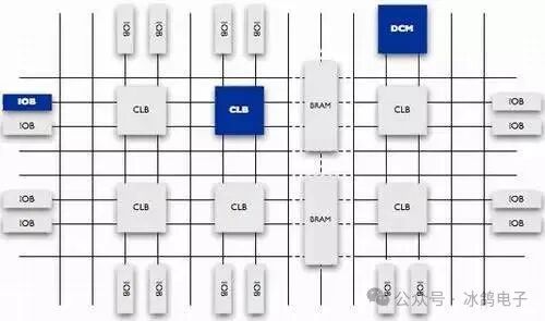
2.1Programmable Input/Output Units (IOB)
The IOB of the FPGA is divided into several groups (banks), and the interface standard of each bank is determined by its interface voltage VCCO. A bank can only have one VCCO, but different banks can have different VCCOs. Only ports with the same electrical standards can be connected together, and having the same VCCO voltage is a basic condition for the interface standard.
2.2Configurable Logic Blocks (CLB)
CLB is the basic logic unit within the FPGA. The actual number and characteristics of CLBs vary depending on the device, but each CLB contains a configurable switch matrix, which consists of 4 or 6 inputs, some selection circuits (multiplexers, etc.), and flip-flops. The switch matrix is highly flexible and can be configured to handle combinational logic, shift registers, or RAM.
In Xilinx FPGA devices, a CLB is composed of multiple (generally 4 or 2) identical slices and additional logic. Each CLB module can be used to implement combinational logic, sequential logic, and can also be configured as distributed RAM and distributed ROM.
A slice is the basic logic unit defined by Xilinx, consisting of two 4-input functions, carry logic, arithmetic logic, storage logic, and function multiplexers.
2.3Digital Clock Management Module (DCM)
Xilinx’s advanced FPGAs provide digital clock management and phase-locked loops. Phase-locked loops can provide precise clock synthesis, reduce jitter, and achieve filtering functions.
2.4Embedded Block RAM (BRAM)
Most FPGAs have embedded block RAM, which greatly expands the application range and flexibility of FPGAs. Block RAM can be configured as single-port RAM, dual-port RAM, content-addressable memory (CAM), and FIFO, among other common storage structures.
2.5Rich Routing Resources
FPGA chips have rich routing resources, which can be divided into four different categories.
The first category is global routing resources, used for global clock and global reset/set routing within the chip;
The second category is long line resources, used for high-speed signals and secondary global clock signal routing between chip banks;
The third category is short line resources, used for logic interconnections and routing between basic logic units;
The fourth category is distributed routing resources, used for dedicated clock, reset, and other control signal lines.
2.6Embedded Lower-Level Functional Units
Embedded functional modules mainly refer to DLL (Delay Locked Loop), PLL (Phase Locked Loop), DSP, and soft processing cores. DLL and PLL have similar functions, capable of achieving high-precision, low-jitter clock multiplication and division, as well as duty cycle adjustment and phase shifting.
2.7Embedded Dedicated Hard Cores
To improve FPGA performance, chip manufacturers integrate some dedicated hard cores within the chip. For example, to enhance the multiplication speed of FPGAs, mainstream FPGAs integrate dedicated multipliers; to accommodate communication buses and interface standards, many high-end FPGAs integrate serial/parallel transceivers (SERDES), achieving transceiving speeds of several tens of Gbps.
Note: Concepts of Soft Cores, Hard Cores, and Firm Cores
IP (Intellectual Property) cores are a general term for integrated circuit cores with intellectual property rights, which are verified macro modules with specific functions, independent of chip manufacturing processes, and can be ported to different semiconductor processes.
Based on the way IP cores are provided, they are usually divided into three categories: soft cores, hard cores, and firm cores. In terms of the cost of completing IP cores, hard cores are the most expensive; in terms of flexibility of use, soft cores have the highest reusability.
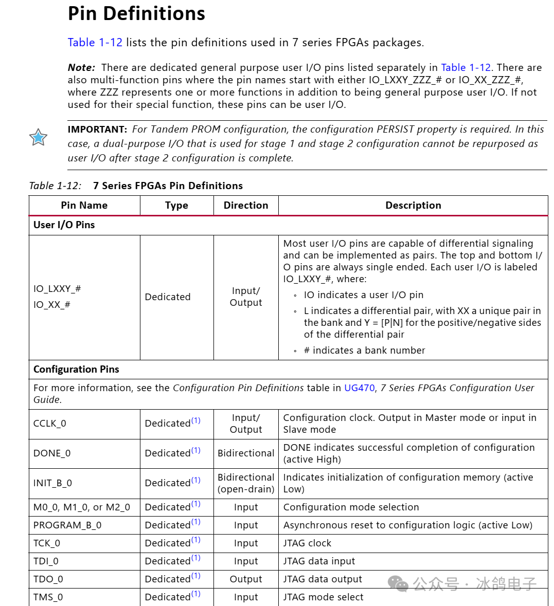
3.Classification of Pins in FPGA
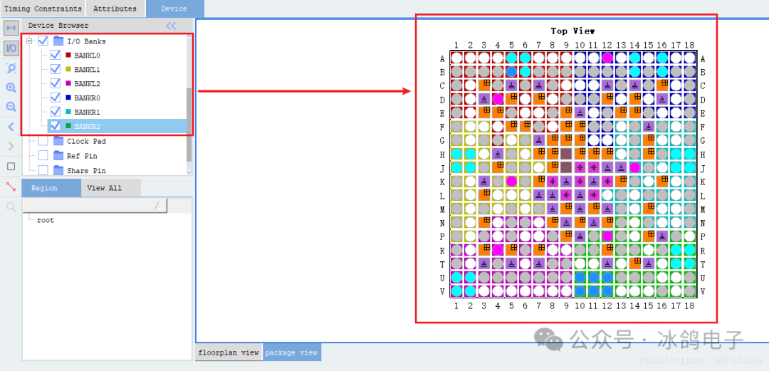
FPGA pins are generally divided into two main categories: dedicated pins (accounting for 20%-30%) and user-defined pins (accounting for 70%-80%), which are further classified based on functionality intoclock, configuration, general I/O, and power four types of pins.
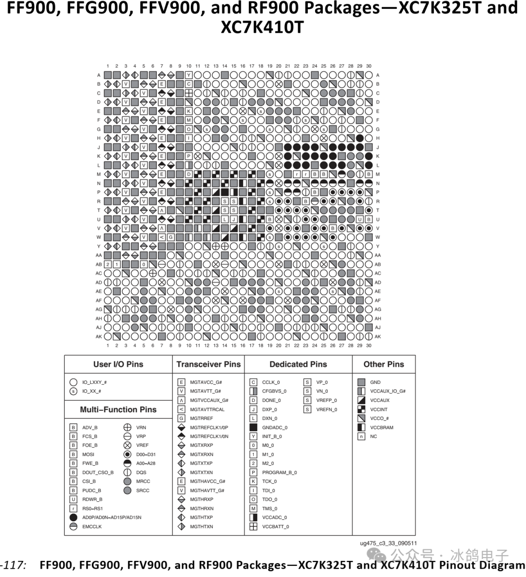
As shown in the figure, identical shapes and markings represent the same type of pin functionality, with power and ground pins generally concentrated in the central area of the chip.
The specific pin definitions can be found in the relevant documentation, usually described in the “Pkg_Pinout” section.
4.Meaning of Banks in FPGA
The programmable input/output unit, referred to as the I/O unit, is the interface part of the chip with external circuits, fulfilling the driving and matching requirements for input/output signals under different electrical characteristics. The I/Os in the FPGA are classified into groups, with each group independently supporting different I/O standards. Through flexible software configuration, it can adapt to different electrical standards and I/O physical characteristics, allowing for adjustments to the driving current and changing pull-up and pull-down resistors.
In Xilinx’s 7 series FPGAs, BANKs are divided into HR (High-range) BANK and HP (High-performance) BANK. HP BANK can only support I/O signals with voltage levels less than or equal to 1.8V, while HR BANK supports I/O signals with voltage levels less than or equal to 3.3V. HP BANK is designed for high-speed I/O signals and supports DCI (Digitally Controlled Impedance), while HR BANK is suitable for more general I/O signal designs.
5.FPGA Power Supply
5.1 Common Power Supply Classifications
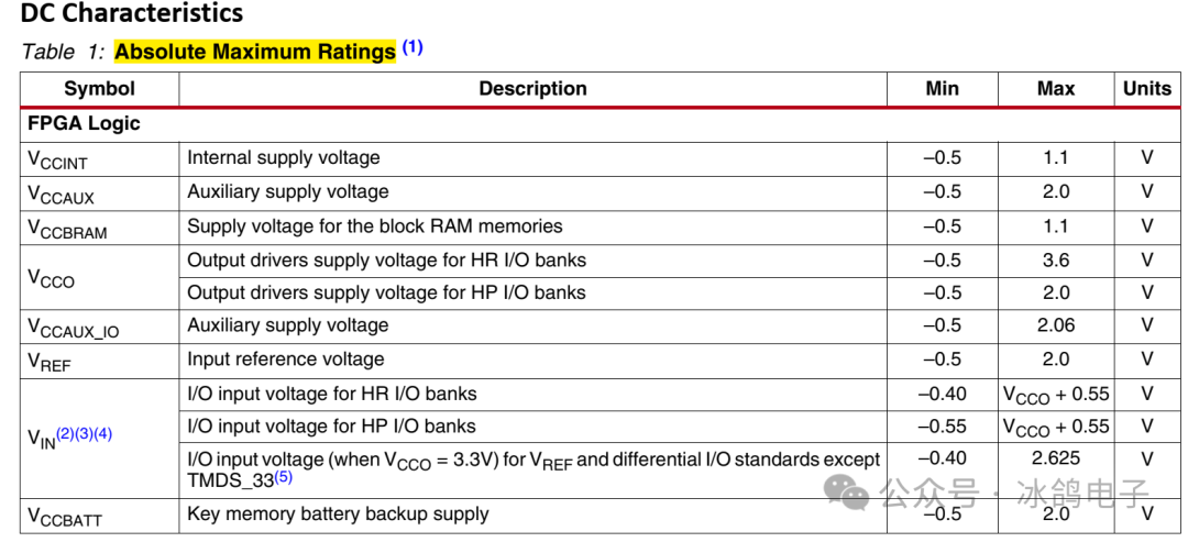
FPGAs typically require at least two voltages to operate: one is the “core voltage,” and the other is the “IO voltage.” Each voltage is supplied through independent power pins.
The core voltage (referred to here as VCCINT) is used to power the logic gates and flip-flops within the FPGA. This voltage has decreased over the years from 5V, 3.3V, 2.5V, 1.8V, to 1.5V as FPGA technology has advanced. The core voltage is fixed (determined by the mode of the FPGA used). The IO voltage (referred to as VCCIO) is the voltage used on the FPGA’s IO modules (same as IO pins). This voltage should match the voltage of other devices connected to the FPGA.
In fact, FPGA devices allow VCCINT and VCCIO to be the same (for example, VCCINT and VCCIO pins can be connected together). However, FPGA designs are oriented towards low-voltage cores and high-voltage I/Os, so these two voltages are generally not the same.
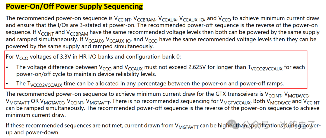
5.2 5.2 Power On/Off Timing Sequence
To ensure that the I/Os remain in a tri-state and operate normally when powered on, the various power rails of the FPGA need to have a specific power-on/power-off timing sequence. Sequential power-up helps limit surge currents during power-up. Ignoring the power supply sequence requirements of the device may lead to damage or latch-up, causing FPGA device failure. This power-on timing sequence will be detailed in the 7 series section.
References: AMD Official Documentation (DS182, UG475, UG471), online articles, etc.