JTAG has 10-pin, 14-pin, and 20-pin configurations. Although the number of pins and their arrangement differ, some pins are the same across these configurations. The definitions of each pin are as follows.
1. Pin Definitions
Test Clock Input (TCK) —– Required 1
TCK is mandated in the IEEE1149.1 standard. TCK provides an independent, basic clock signal for TAP operations, and all TAP operations are driven by this clock signal.
Test Mode Selection Input (TMS) —– Required 2
The TMS signal is valid on the rising edge of TCK. TMS is required by the IEEE1149.1 standard. The TMS signal is used to control the transitions of the TAP state machine. Through the TMS signal, TAP can be controlled to transition between different states.
Test Data Input (TDI) —– Required 3
TDI is required by the IEEE1149.1 standard. TDI is the data input interface. All data to be input to a specific register is serially input one bit at a time through the TDI interface (driven by TCK).
Test Data Output (TDO) —– Required 4
TDO is required by the IEEE1149.1 standard. TDO is the data output interface. All data to be output from a specific register is serially output one bit at a time through the TDO interface (driven by TCK).
Test Reset Input (TRST) —- Optional 1
This signal interface is optional in the IEEE 1149.1 standard and is not mandatory. TRST can be used to reset (initialize) the TAP Controller. Since TAP can also be reset (initialized) through TMS, there are distinctions between four-wire and five-wire JTAG.
(VTREF) —– Required 5
The reference voltage level for the interface signal is generally connected directly to Vsupply. This can be used to determine the logic level used by the ARM JTAG interface (e.g., 3.3V or 5.0V?).
Return Test Clock (RTCK) —- Optional 2
Optional, a clock signal fed back from the target to the emulator, used to synchronize the generation of TCK signals; if not used, it should be grounded.
System Reset (nSRST)—- Optional 3
Optional, connected to the system reset signal on the target board, can directly reset the target system. It can also detect the reset state of the target system; to prevent false triggering, a suitable pull-up resistor should be added on the target side.
USER IN
User-defined input. Can be connected to an IO for receiving control from the host computer.
USER OUT
User-defined output. Can be connected to an IO for providing feedback of a status to the host computer.
Since JTAG is often connected via ribbon cables, to enhance anti-interference capability, ground lines are added between each signal line, resulting in this 20-pin interface. However, in practice, RTCK, USER IN, and USER OUT are generally not used, leading to the existence of a 14-pin interface. For practical development applications, due to the stable laboratory power supply and good electromagnetic environment, interference is minimal.
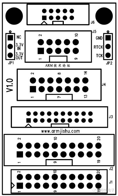
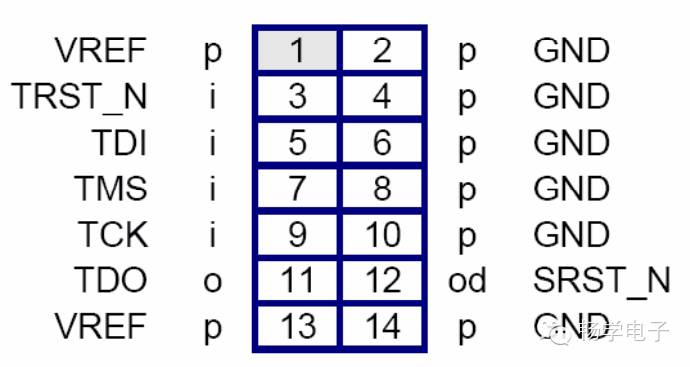
2. Correspondence between Pin Names and Numbers for 20, 14, and 10-pin JTAG
It is worth noting that different IC companies define their proprietary JTAG headers for downloading or debugging programs. The signal arrangements for the commonly used 20, 14, and 10-pin JTAG in embedded systems are as follows: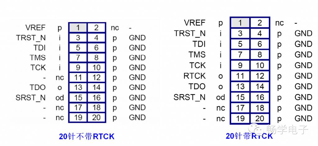
It should be noted that the pin names of the above JTAG headers are relative to the IC. For example, the TDI pin indicates that this pin should be connected to the TDI pin on the IC, rather than indicating that data enters the download cable from this pin.
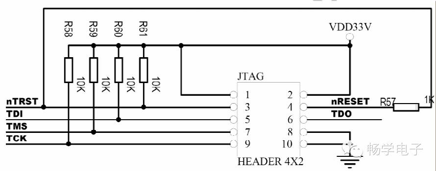
In fact, only 4 wires need to be connected for the 10-pin configuration; pin 4 is a self-loop and does not need to be connected; pins 1 and 2 connect to pin 1, while pins 8 and 10 connect to GND, which can also be left unconnected.
Attached is the circuit of the adapter board: