
This article will explain the composition of PCBs in detail, as well as some commonly used terms in the PCB field, a brief assembly method, and an overview of the PCB design process.
01Birth of PCBBefore the advent of PCBs, circuits were composed of point-to-point wiring, which had low reliability. As circuits aged, wire breakage could lead to open or short circuits at the junctions.Wiring technology was a significant advancement in circuit technology, enhancing the durability and replaceability of connections by winding small diameter wires around the pillars at connection points.As the electronics industry transitioned from vacuum tubes and relays to silicon semiconductors and integrated circuits, the size and cost of electronic components also decreased.With electronic products increasingly appearing in the consumer sector, manufacturers sought smaller and more cost-effective solutions, leading to the birth of PCBs.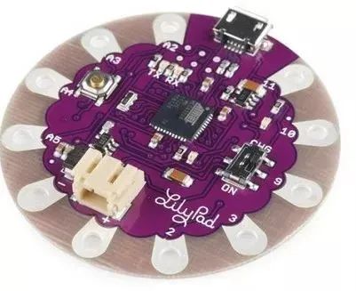 02Composition of PCBPCBs resemble multi-layer cakes or lasagna—different layers of materials are pressed together using heat and adhesives during production.
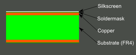 03PCB SubstrateThe substrate of a PCB is generally made of fiberglass, most commonly referring to FR4 material, which provides rigidity and thickness to the PCB.In addition to FR4, flexible circuit boards can be produced on flexible high-temperature plastics (such as polyimide).
 Cheap PCBs and perfboards (see above) are made from materials like epoxy resin or phenolic, lacking the durability of FR4 but are much cheaper. When soldering on these boards, a strong odor will be noticeable.This type of substrate is often used in very low-end consumer products, as phenolic materials have a lower thermal decomposition temperature. Prolonged soldering can lead to decomposition and carbonization, emitting an unpleasant smell.04Copper Foil
 Next, we introduce the very thin copper foil layer, which is pressed onto the substrate using heat and adhesive during production. In double-sided boards, copper foil is pressed onto both sides of the substrate.In some low-cost scenarios, copper foil may only be pressed onto one side of the substrate. When we refer to “double-sided boards” or “two-layer boards,” we mean that our lasagna has two layers of copper foil.Of course, in different PCB designs, the number of copper foil layers can be as few as one or more than sixteen.There are various thicknesses of copper layers, typically measured in ounces (oz) per square foot, indicating the weight of copper uniformly covering one square foot.Most PCBs have a copper thickness of 1oz, but some high-power PCBs may use 2oz or 3oz of copper thickness, which translates to approximately 35um or 1.4mil of copper thickness per ounce (oz) per square foot.05Solder MaskOn top of the copper layer is the solder mask layer, which gives the PCB its green or SparkFun red appearance.The solder mask covers the traces on the copper layer, preventing them from contacting other metals, solder, or other conductive objects, which could cause short circuits.The presence of the solder mask allows for soldering in the correct places and prevents solder bridging.
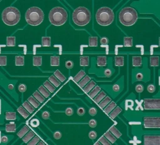 As shown in the image above, we can see that the solder mask covers most of the PCB, including the traces, but exposes the silver holes and SMD pads for easy soldering. Generally, the solder mask is green, but almost any color can be used for solder masks.06Silkscreen
 Above the solder mask layer is the white silkscreen layer, which prints letters, numbers, and symbols on the PCB to facilitate assembly and help users better understand the board’s design.We often use symbols on the silkscreen layer to indicate the functions of certain pins or LEDs. The most common color for the silkscreen layer is white, but it can be made in almost any color.Black, gray, red, and even yellow silkscreen layers are not uncommon, but it is rare to see multiple colors of silkscreen layers on a single board.07TerminologyNow that you know the structure of a PCB, let’s take a look at some PCB-related terminology.Pad Ring:The copper ring around the metallized hole on the PCB.
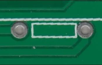 DRC:Design Rule Check, a program that checks for errors in the design, such as short traces, traces that are too thin, or holes that are too small.Drill Hit:Indicates the deviation between the required drill hole position in the design and the actual drill hole position. Incorrect drill centers caused by dull drill bits are a common issue in PCB manufacturing.
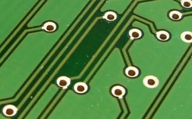 As shown in the image above, this is a somewhat inaccurate drill hit illustration.Gold Finger:Exposed metal pads on the edge of the board, typically used to connect two circuit boards, such as the edges of computer expansion modules, memory sticks, and older game cartridges.Stamp Hole:Another optional board separation design method, using a series of continuous holes to form a weak connection point, allowing the board to be easily separated from the panel.
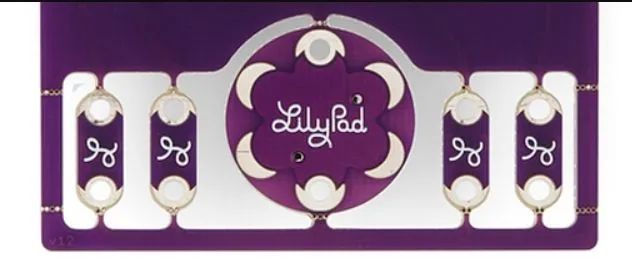 Pad:A portion of exposed metal on the surface of the PCB used for soldering components.
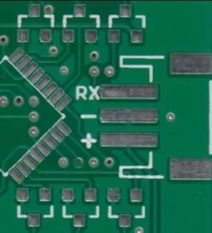 Panel:A large circuit board composed of many smaller, separable circuit boards. Automated circuit board production equipment often encounters issues when producing small boards, so combining several small boards can speed up production.Stencil:A thin metal or plastic template used during assembly to allow solder paste to pass through specific areas on the PCB.
 Pick-and-Place:A machine or process that places components onto the circuit board.Plane:A continuous copper area on the circuit board, generally defined by boundaries rather than paths, also known as copper pour.
 Metalized Via:A hole on the PCB that includes a pad ring and plated hole walls. Metalized vias can serve as connection points for plugs, signal layer transitions, or mounting holes.
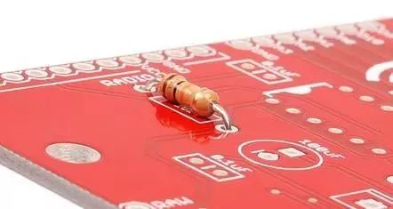 FABFM A plug resistor on the PCB, with its two legs passing through the via, allowing the plated hole walls to connect traces on both sides of the PCB.Pogo Pin:Refers to a spring-loaded temporary contact point, typically used for testing or programming.
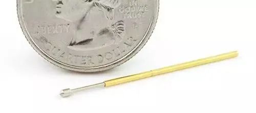 Reflow Soldering:Melting solder to connect SMD pads and component pins together.Slot:Refers to any non-circular hole on the PCB. Slots can be plated or unplated. Since slots require additional cutting time, they may increase the cost of the board.
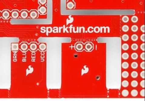 Note: Due to the circular nature of the slot cutting tool, the edges of the slot cannot be made perfectly square.Solder Paste Layer:Before placing components on the PCB, a certain thickness of solder paste is formed on the SMD pads through a stencil.During the reflow soldering process, the solder paste melts, establishing a reliable electrical and mechanical connection between the pads and component pins.
 Before placing components, a brief solder paste layer on the PCB; remember to learn about the definition of stencils.Soldering Furnace:A furnace for soldering plug-in components, typically containing a small amount of molten solder. The board quickly passes over it to solder the exposed pins.Solder Mask:A protective layer covering the copper to prevent short circuits, corrosion, and other issues.
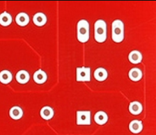 Cold Solder:Two connected pins on a component mistakenly connected by a small drop of solder.Surface Mount:A method of assembly where components are simply placed on the board without needing to pass their pins through holes.Thermal Pad:Refers to a short trace connecting a pad to a plane. If the pad is not designed for proper heat dissipation, it can be difficult to heat the pad to the required soldering temperature during soldering, leading to a sticky pad and longer reflow times.
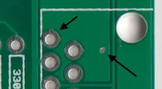 On the left, the pad is connected to the ground plane through two short traces (thermal pads). On the right, the via connects directly to the ground plane without using a thermal pad.Trace:A generally continuous copper path on the circuit board.
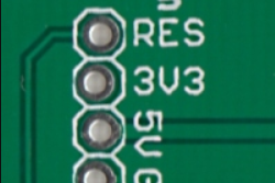 A trace connecting the reset point to other locations on the board, with a relatively thicker trace connecting to the 5V power point.V-score:A method of making an incomplete cut on the board, allowing it to be broken along this line.Via:A hole on the board, generally used to switch signals from one layer to another.Plug holes refer to vias covered with solder mask to prevent soldering. Since connectors or component pins require soldering, they are generally not plugged.
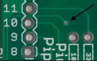 Both sides of the same PCB with plugged vias, allowing signals from the front to be transmitted to the back through drilled holes on the board.
Wave Soldering:A method of soldering plug-in components, where the board is passed uniformly through a molten solder furnace that generates a stable wave peak, soldering the component pins to the exposed pads.

Some screenshots from electronic books
【Complete Set of Hardware Learning Materials】