
This chapter introduces some technologies that design Gallium Nitride (GaN) for power amplifiers (PAs) and other applications, describing how GaN is widely used in RF (Radio Frequency) front ends. We also explore how technology leaders provide discrete, monolithic microwave integrated circuits (MMICs), and highly integrated modules to accommodate multiple application areas. Additionally, we explain the important aspects and advantages of GaN thermal modeling in applications.
1. Design Using Gallium Nitride
Traditionally, GaN power amplifier designs primarily rely on approximate starting points and a wealth of experience and expertise. Utilizing S-parameters and load pull data can effectively enhance the success rate of designs. For discrete device solutions, employing precise nonlinear models can generate design data more quickly. During the implementation of discrete devices, modeling helps to simulate semiconductor behavior more accurately, achieving better design outcomes for specific applications.
For engineers, the first step in designing GaN power amplifiers is to consult the product data sheets from semiconductor manufacturers, followed by analyzing S-parameters. Designers can also obtain optimal load impedance targets corresponding to specific frequency power and efficiency values through measured load pull data. Combining load pull data with simulation models (when available) can help designers achieve more desirable results. Figure 3-1 illustrates the process of constructing simulation models in GaN power amplifier design, which are also used to generate power amplifier reference designs.
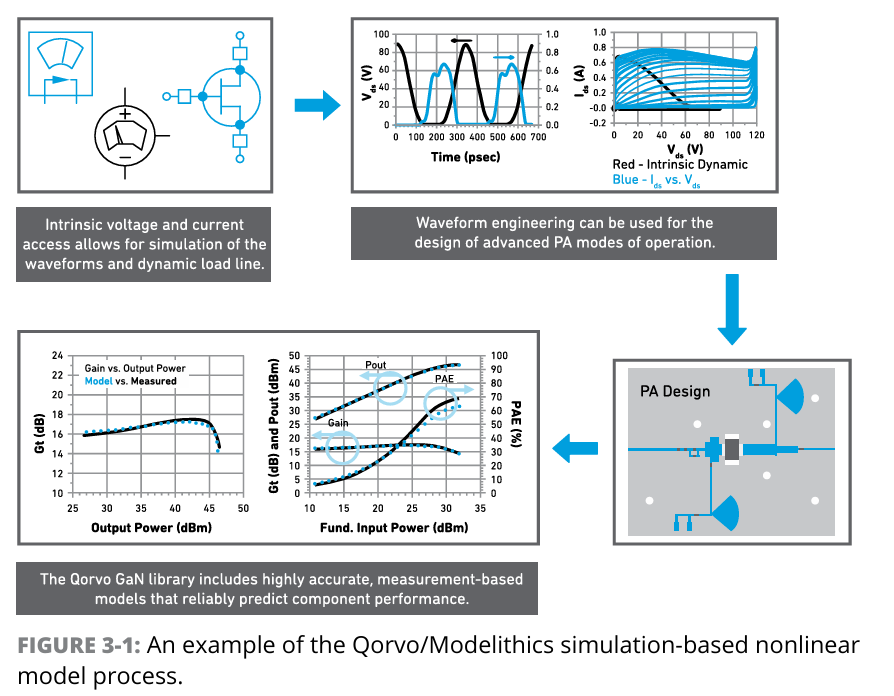
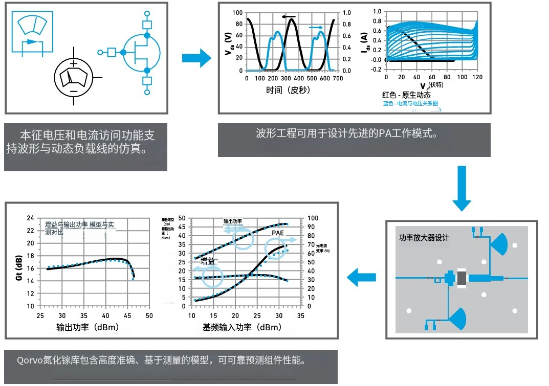
These discrete nonlinear GaN models possess the following characteristics: adjustable bias, temperature scaling effects, self-heating effects, intrinsic current-voltage sensing capabilities, and suitable bond wire configurations. At the most basic level, nonlinear transistor GaN models must capture the current-voltage characteristics (I-V curves) of the transistor at different operating levels, which directly determine the core power, efficiency, and other key performance drivers of the device.
The model’s ability to predict the nonlinear behavior of power amplifier transistors depends on several key factors:
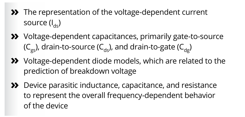
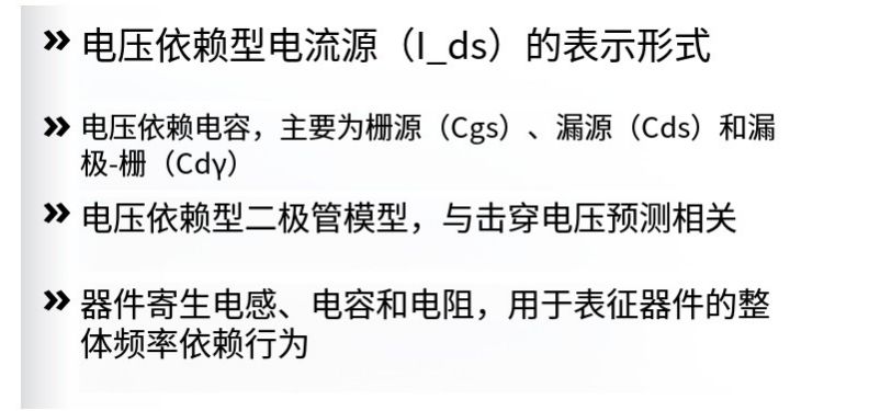
As a relatively new technology, GaN requires some different modeling and design approaches compared to other semiconductors. GaN effectively expands the boundaries of the I-V curve due to its higher maximum current capability, higher static operating voltage, and ability to operate at higher voltages. Nevertheless, data must be provided to engineers so they can optimize their designs under target application voltage, current, and load conditions. This data can accelerate the design process and help engineers achieve the correct layout on the first attempt without worrying about costly project rework.
2. GaN and RF Front Ends
In the early development of GaN, it was primarily used for the transmit signal amplification stage of RF front ends, mostly appearing in chip form or transistors with flanges. However, using GaN for other RF front end components also has significant advantages. Today, GaN is also used in low-noise amplifiers, mixers, and switches—both as discrete components and as monolithic microwave integrated circuits. This section will review the advantages of GaN in these RF front end components.
2.1 GaN Power Amplifiers
For the power levels and efficiency required for most high-power applications, GaN is an obvious choice. It can provide high durability and high saturation power within a very small size range. At the same time, it meets the high efficiency required for many wireless base stations, commercial, and military radar applications.
2.2 GaN Switches
GaN switches are suitable for many RF switch applications. They have high breakdown voltages and combine low on-resistance and off-state capacitance characteristics. This significantly enhances power handling capability.
Gallium Arsenide (GaAs) field-effect transistor switches are widely used in the RF industry, typically suitable for power levels of a few watts or lower. In contrast, GaN FETs can handle much higher power levels of tens of watts using the same circuit architecture. GaN switches offer low switching losses, high isolation, high linearity, and excellent power handling capabilities. As the system demand for higher current, voltage capability, power density, temperature, efficiency, and frequency range continues to grow, silicon-based switches are gradually approaching their performance limits. Therefore, GaN switches are replacing silicon-based switches in applications that require these unique capabilities.
2.3 GaN Low Noise Amplifiers
Compared to other LNA technologies, GaN LNAs typically consume less power. Choosing GaN for LNA manufacturing can provide low noise figures and the high input power robustness required by LNAs.
Typically, GaN devices can withstand input power levels of 2 to 4 watts. This high input power tolerance is particularly important in many applications. For example, in many radar applications, one way to mitigate the impact of high input power on the receiver is to add a limiter or circulator at the input. This helps provide protection but has the side effect of increasing noise at the LNA. This limiter or circulator solution also reduces the sensitivity of the receiver, negatively impacting signal range, throughput, and performance. In contrast, the extremely high input power tolerance of GaN LNAs means that limiters or circulators are no longer necessary, thus helping to improve overall receiver performance.
2.4 GaN Mixers
GaN-based mixers have high linearity and can handle higher input power than GaAs-based mixers. Typically, these high-end GaN-based mixers are used in defense, satellite communications, and instrumentation applications.
The advent of GaN technology provides design engineers with another technology option for designing RF front ends. This new technology brings more opportunities.
3. GaN System Reliability Assessment
It is well known that GaN is more reliable than other technologies, primarily due to its unique properties: reliable high power handling capability and thermal robustness. Nevertheless, it is crucial for designers to create robust solutions around this technology to achieve optimal system-level reliability.
As with all power transistor technologies, careful thermal design is critical to ensuring reliable operation. The key to supporting high voltage and high efficiency is to remove heat from the device, keeping the junction temperature within an acceptable range for reliable operation. This can be achieved through precise thermal measurements and selecting substrate materials with the best thermal performance that can instantly conduct heat from the device to the heat sink.
One alternative thermal solution for heat sinks is copper core technology. This method embeds metal blocks into the printed circuit board during manufacturing, allowing for efficient heat transfer from the transistor to the PCB-mounted carrier. Compared to more expensive heat sinks or fans, this method provides better thermal transfer at a lower cost.
Although copper core cooling can significantly improve device temperature, it has a slight impact on RF performance. Additionally, care must be taken to ensure that the PCB remains flat and that there is good contact between the copper core and the ground pad of the device package.
4. Comparison of GaN and Traveling Wave Tube Amplifiers
As shown in Table 3-1, GaN processes use commercial materials and manufacturing platforms that provide optimal reliability, lower costs, and high performance. Therefore, whether it is silicon carbide-based GaN or silicon-based GaN, both offer engineers a more cost-effective, competitive, and reliable solution compared to traditional traveling wave tube amplifier (TWTA) technology.
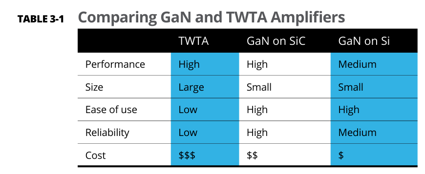
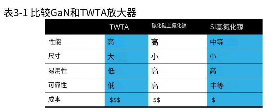
For example, in commercial and military radar applications that require operation in the gigahertz (GHz) frequency range, GaN has proven to be an ideal solution, especially in the transmit stage. It has replaced traveling wave tube amplifiers (TWTA) in many such applications. Today’s military radar using active electronically scanned arrays (AESA) and phased array modules particularly benefit from using GaN, as they can leverage monolithic microwave integrated circuit (MMIC) technology, simplifying design and reducing size.
5. Coordinating GaN Thermal Characteristics with Applications
Increasing power may mean exacerbated thermal management challenges. High operating temperatures can lead to degraded device performance and reduced product lifespan. Therefore, design engineers need to continuously assess thermal impacts to mitigate potential issues at both the device and system levels.
Due to GaN’s excellent thermal characteristics, it is being considered for many applications that need to operate in high temperatures and extreme environments. GaN’s extremely high 225°C channel operating temperature liberates system designers from a thermal design perspective. For example, some applications that require liquid cooling when implemented with laterally diffused metal-oxide semiconductors (LDMOS) or GaAs can switch to air cooling when using GaN.
Although GaN is more heat-resistant than many semiconductor technologies, engineers must still fully understand thermal design and analysis to build robust and reliable final products. A comprehensive understanding of GaN’s thermal characteristics is crucial before product design promotion.
Estimating Maximum Channel Temperature (TCH, MAX)
The reliability of semiconductors like GaN is determined by estimating the device’s maximum channel temperature (TCH, MAX) to confirm its expected lifespan. These values are collected by measuring and modeling thermal resistance, device power consumption, and heat transfer. For semiconductor devices, measurements are primarily conducted using infrared (IR) imaging microscopes. These infrared (IR) imagers help identify hotspots on the device that may ultimately lead to failure areas on the semiconductor.
Because GaN technology can operate at higher temperatures than most semiconductor materials, it is crucial to measure channel temperature more accurately. Therefore, some GaN designers and semiconductor manufacturers choose to conduct additional measurements beyond infrared scanning.
Why? The accuracy of infrared (IR) imaging in measuring GaN channel temperature is limited due to factors such as spatial resolution limitations, difficulties in imaging reflective surfaces, and the influence of chip surface structures (like air bridges). Furthermore, even if accurate infrared image values are obtained, the true maximum channel temperature (TCH, MAX) is actually located beneath the device gate, as shown on the right side of Figure 3-2.
To obtain more accurate channel temperature measurements, one method is to use a thermal modeling analysis method called finite element analysis (FEA). Combining three-dimensional modeling (3D Modeling) or finite element analysis (FEA) with micro-Raman thermography and comparing these results with RF testing and infrared imaging can provide accurate thermal parameter values. Using this combined dataset, the finite element analysis (FEA) model of the package components can be determined, revealing the true maximum channel temperature (TCH, MAX). Additionally, as shown on the left side of Figure 3-2, compared to infrared image spot size measurements, micro-Raman spot size measurements can provide much more precise temperature measurements at different locations beneath the gate. This offers a more accurate method for measuring peak channel temperature.
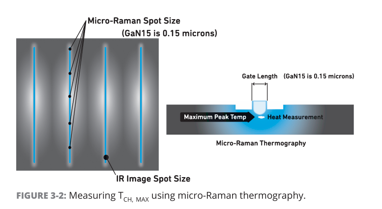
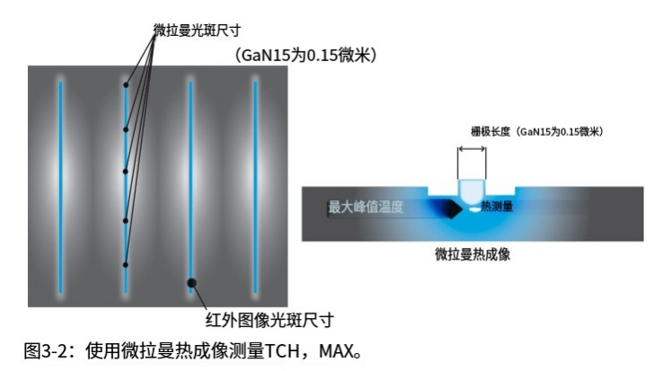
Micro-Raman thermography is a non-destructive optical technique based on Raman scattering spectroscopy that enables temperature measurements with sub-micron spatial resolution and nanosecond time resolution. This technique works by detecting phonon shifts in the material caused by temperature changes (relative to the reference phonon frequency measured at ambient temperature).
To calculate the expected lifespan of the device, determining its true maximum channel temperature (TCH, MAX) is a multi-step process. First, by performing three-dimensional thermal modeling (3D thermal modeling) or finite element analysis (FEA) and comparing it with empirical measurement data, including micro-Raman thermography, to determine channel temperature. Subsequently, verification is conducted through RF (Radio Frequency) testing and infrared (Infrared, IR) imaging, utilizing the combined data to obtain accurate measurements of GaN channel temperature and device reliability.
Finite element analysis (FEA) is a comprehensive method for measuring the true channel temperature of GaN and assessing device reliability. It employs a three-pronged strategy, utilizing data from component backside temperature, chip or component attachment measurements, and infrared (IR) imaging to create a finite element analysis (FEA) model, accurately estimating the lifespan of GaN devices.
View the Operating ProcedureWant to learn more about this method? Watch the tutorial video “Understanding GaN Thermal Analysis” at www.qorvo.com/design-hub/videos/understanding-gan-thermal-analysis.
Continuous Wave vs. Pulsed Operating ModesAnother important design and reliability factor to consider is how GaN devices operate in the system. Are the devices continuously on (Continuous Wave [CW] operation) or pulsed switches (Pulsed Wave operation)? These operating modes affect the maximum channel temperature (TCH, MAX) values, which depend on specific operating conditions and vary with the selected pulse width and duty cycle. For example, after the system reaches thermal steady-state operation, the maximum channel temperature (TCH, MAX) under continuous wave (CW) operation is at its highest.
6. Evaluating GaN Packaging Forms
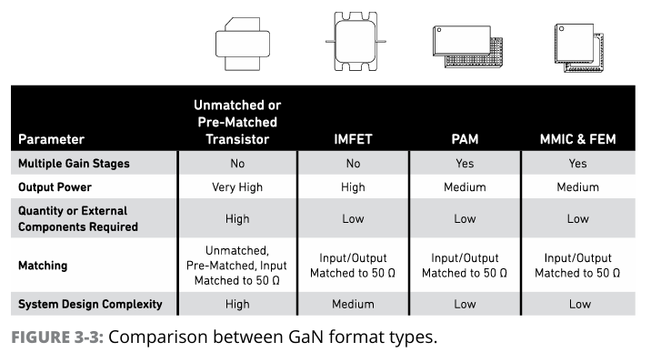
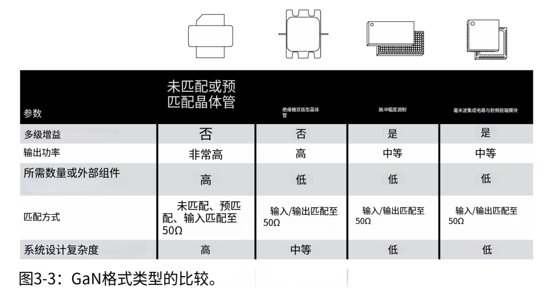
GaN offers chip form and various packaging formats: prematched transistors, internally matched field-effect transistors (IMFETs), power amplifier modules (PAMs), or monolithic microwave integrated circuits (MMICs). As shown in Figure 3-3, each form has its advantages and trade-offs.
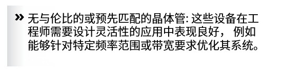
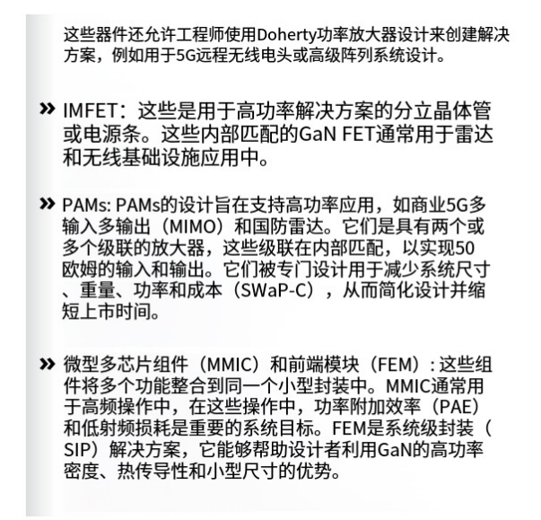
For specific applications, each form can provide top-notch thermal performance, size, and parameter performance. Below is a brief description of the use cases for these GaN form types:
7. Exploring GaN System Design and Implementation
Mature technologies like GaAs can support large bandwidths and high frequency bands, but their power density is lower than that of GaN. Therefore, in applications where unit transmit power requirements are lower and receiver chain noise figure is a critical metric, GaAs high electron mobility transistors remain a viable solution for transmit and receive components.
The continuous reduction of GaAs gate lengths helps to lower noise figures, thereby improving RF range and sensitivity. All else being equal, reducing GaAs gate lengths helps enhance performance, but this comes at the cost of electrostatic discharge tolerance and input power survivability. However, compared to GaAs, silicon carbide-based GaN not only has higher input power (which helps improve survivability) and lower noise figures but also offers wide bandwidth and higher power density advantages. Additionally, GaN’s high input impedance makes it easier to achieve RF matching in systems.
Using higher power density GaN transistors can simplify designs and reduce the number of matching components in the system. This also means fewer overall system components are used, thereby reducing RF chain losses compared to GaAs and laterally diffused metal-oxide semiconductors. With GaN’s higher transmit power and lower receive noise figures, systems can achieve longer RF distances and higher signal resolution.
In radar applications, this means that systems can detect smaller targets at greater distances, providing longer reaction times to target movements. Traditional radar systems require short pulse widths, narrow instantaneous bandwidths, and small duty cycles. However, today, all radar bands are pushing to increase duty cycles three to five times, reaching 50% or higher—in some cases approaching continuous wave operation.
Radar active electronically scanned array systems may use hundreds to thousands of amplifiers. With GaN technology, it is possible to increase the power of each array unit to enhance detection range while using fewer GaN devices compared to GaAs and other technologies to achieve the required output power, thus reducing costs and complexity.
GaN power amplifiers have the highest efficiency in the saturation region. However, linearity is quite the opposite: the most linear operating region is at lower or back-off output power levels. In 5G systems, linearity is a key parameter. Therefore, to maximize linearity in high-power 5G advanced antenna systems, a technique called digital predistortion is employed (see Figure 3-4).
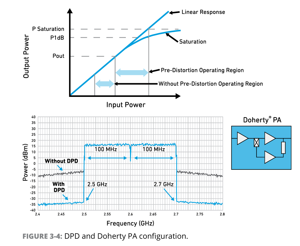
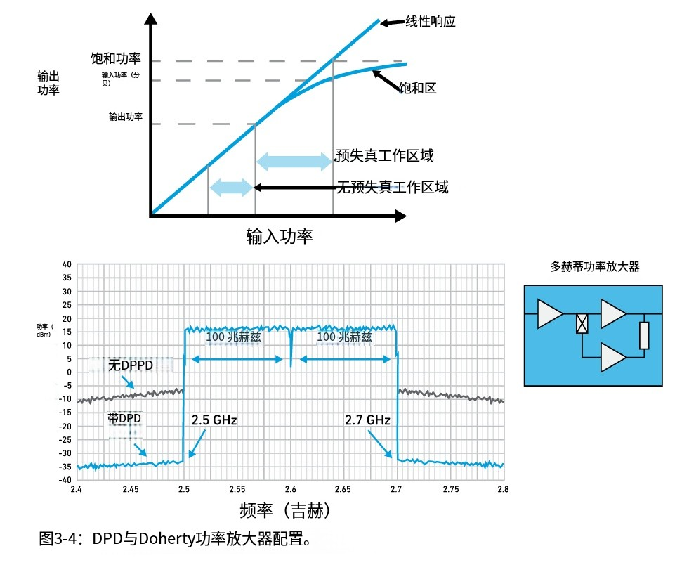
Power amplifiers in 5G base stations are typically optimized for efficiency, requiring power-added efficiency to reach 50% to 70%. Linearity is compensated for through digital predistortion technology. Efficiency is critical because the signal output power and associated energy consumption are high. Another advantage is that these systems operate at lower temperatures, which is particularly important as they are installed at the top of base station antennas rather than indoors with air conditioning at the building’s bottom.
Digital predistortion is a hardware and software-based solution that eliminates distortion through digital signal processing techniques. It enables designers to optimize power amplifiers for lower power consumption while maximizing output power and achieving high linearity.
8. Examining GaN Doherty Power Amplifiers and Digital Predistortion Technology
In certain innovative RF systems, such as 5G base stations, the industry is striving to enhance the output levels, efficiency, and linearity of power amplifiers. To effectively achieve these three parameters simultaneously, digital predistortion technology is highly beneficial. This technology also minimizes out-of-band distortion generated by power amplifiers.
Many GaN power amplifiers adopt a Doherty architecture to enhance device efficiency in power back-off states. Through this configuration, engineers can minimize system power consumption and achieve efficiencies of 60% or higher (in power back-off states), significantly reducing the operational energy consumption of high-power power amplifier systems. When employing a Doherty architecture, digital predistortion is indispensable. As shown in Figure 3-4, the combination of digital predistortion and the Doherty architecture can achieve higher efficiency and linearity.
9. High Voltage GaN Technology Analysis
For certain applications, achieving the highest possible output power is crucial. As mentioned earlier, power amplifiers are most efficient when approaching saturation or peak output power. Increasing the drain voltage of GaN transistors can achieve higher power output in saturation. However, this technology may be suitable for specific applications but not universally applicable.
Radar is a typical application area where high voltage GaN opens a new era. Radar systems typically require hundreds to thousands of watts of power amplification capability. Traditionally, this has been achieved by combining multiple solid-state power transistors or using traveling wave tube amplifiers to achieve kilowatt-level amplification.
GaN technology can achieve these output power levels with fewer transistors due to its higher operating voltage. For example, at a 65-volt operating voltage, GaN can achieve kilowatt-level amplification while maintaining lower heat dissipation requirements. Additionally, compared to other technologies, it can meet military target parameters for identification and ranging with a smaller footprint, more reliable performance, and fewer transistors.
As an added advantage, high voltage GaN effectively reduces design complexity by decreasing the number of transistors required to achieve high power levels. These high-voltage high-power transistors also exhibit high efficiency characteristics, achieving efficiencies of 70% to 80% in some cases.
Here are some key advantages of high voltage GaN:

Currently, GaN device designs target drain bias voltages of 28-32V, 48-50V, or 65V (see Figure 2-2), but to achieve superior performance advantages in systems, the industry is exploring higher operating voltage ranges for emerging and existing markets.
Appendix:
“Approximate starting points” refer to the imprecise, experience-based, or rough estimates that engineers rely on when designing GaN power amplifiers.It can be understood as an “educated guess.” It is not an optimal solution derived from precise calculations or simulations, but rather a generally correct starting point adopted to initiate the design process.
Specifically, in PA design, these “approximate starting points” may include:
-
Initial impedance values based on classical theory: For example, the load impedance calculated using the ideal impedance formula for transistors (such as
<span>Ropt = (Vdd - Vknee) / Imax</span>). This value does not consider the parasitic parameters of the actual device (such as package inductance, capacitance), frequency discretization effects, etc., so it is an approximation. -
Values borrowed from similar designs: Engineers may infer the initial bias point or matching circuit topology for GaN designs based on previous designs of silicon-based or GaAs amplifiers at similar frequencies or power levels. Due to material differences, these borrowed values can only be “approximate.”
-
“Rules of thumb” or empirical formulas: Some simplified calculation rules summarized from long-term industry practice. These rules are easy to use but have limited accuracy.
-
Typical values in data sheets: Data sheets may provide a “typical” load impedance under specific conditions (such as a single frequency, fixed bias). However, this condition may not match your specific design goals, so it can only serve as a starting point.
Why do traditional methods rely on “approximate starting points”?Because in an era without precise nonlinear models and powerful simulation tools, designing entirely from scratch and finding the optimal solution through pure theoretical calculations is very difficult and time-consuming. Therefore, engineers utilize their knowledge and experience to establish a “generally correct” initial design, which is then refined throughextensive manual tuning, prototyping, and testing to ultimately meet requirements. This process heavily relies on “expert knowledge.”
In contrast, the modern methods (mentioned in the text) are:
-
Using S-parameters: Conducting small-signal linear analysis to help design stable amplifiers and provide initial matching references.
-
Using load pull data: Directly measuring experimentally to find the precise load impedance that the transistor needs to “see” for optimal output power or efficiency. This is much more accurate than any “approximate starting point.”
-
Using precise nonlinear models: In simulation software, utilizing complex models that can simulate the nonlinear behavior of transistors to directly generate the data needed for various designs (such as I-V curves, load pull profiles), thus skipping the “guessing” phase and starting the design from a better point.
To summarize:
“Approximate starting points” are a “rough draft,” while modern design methods utilize advanced tools and data to aim for a “refined draft,” significantly reducing subsequent debugging workload and uncertainty, thereby improving design success rates.
-
Doherty Power Amplifier
-
Objective: To address the core issue of efficiency sharply declining in power amplifiers during power back-off.
-
Principle: Two amplifiers (carrier amplifier and peak amplifier) work together through load modulation techniques. Its core advantage is that it can achieve high efficiency at both peak power and approximately 6dB back-off (i.e., one-quarter of peak power).
-
Value: As modern communication signals (such as OFDM used in 5G) have a high peak-to-average power ratio, amplifiers are not operating at peak power most of the time. The Doherty structure significantly enhances the system’s average efficiency, thereby greatly reducing base station energy consumption and heat dissipation requirements.
Digital Predistortion
-
Objective: To address the nonlinear distortion issues of power amplifiers.
-
Principle: DPD is a technique based on digital signal processors and software algorithms. It pre-injects a distortion that is “opposite” to the amplifier’s distortion characteristics before sending the signal to the power amplifier. Thus, when the signal passes through the nonlinear amplifier, the two distortions cancel each other out, ultimately outputting a clean, linear signal.
-
Value: Ensures that the transmitted signal meets strict spectral mask requirements, preventing interference with other channels and ensuring modulation quality, thereby enhancing system capacity and throughput.
Why must they be used together?
When using Doherty, DPD is essential. This is key for the following reasons:
-
Inherent trade-off between efficiency and linearity: Power amplifiers have a fundamental trade-off in design: the closer they operate to saturation (high efficiency region), the stronger their nonlinearity becomes. The Doherty structure inadvertently exacerbates nonlinear distortion by allowing the amplifier to operate in a more efficient state.
-
Complexity of the Doherty architecture: Traditional DPD algorithms are designed for single amplifiers. However, Doherty amplifiers have two amplifiers whose on and off states change with input power, making it a more complex, dynamic nonlinear system. Ordinary DPD algorithms struggle to accurately model and correct this complex distortion behavior.
-
Ultimate requirements for system performance: To simultaneously meet the stringent requirements for high efficiency and high linearity in systems like 5G, both must be combined.
-
Doherty PA is responsible for achieving efficient power conversion.
-
Advanced DPD is responsible for “fixing” the distortion caused by high-efficiency operation, ensuring signal quality.
Benefits of Collaborative Operation
As shown in the figure below, when both are perfectly combined, the system can achieve:
-
Higher average efficiency: Thanks to the Doherty structure, operational costs are reduced.
-
Excellent linearity: Thanks to DPD, signal quality and spectral efficiency are improved.
-
Wider dynamic range: The system can maintain good performance over a wider power range.
Conclusion
Doherty Power Amplifiers and Digital Predistortion are a complementary “golden pair.” The Doherty PA provides the system with a “robust physique” (high energy efficiency), while DPD gives it “precise control” (high linearity). In high-demand applications like 5G base stations, both are indispensable. Without DPD, the distortion generated by the Doherty PA would render it impractical; without the Doherty PA, the system would struggle to handle the high energy consumption of 5G. Their combination is a core technological pillar for achieving green, high-performance communication networks.