
Click to follow me
In the complex process of chip manufacturing, tape-out is a crucial step, representing a thrilling leap from design blueprint to actual application. Tape-out, known in English as “Tape-out”, refers to the process of delivering the design plan (GDSII file) to the wafer fabrication plant for trial production after the chip design is completed. This process aims to produce a small number of samples (usually only a few dozen) for testing and verifying the correctness, functionality, and performance of the design. The importance of tape-out is self-evident. It is the key transition from chip design to physical product, directly determining whether the chip design can successfully transform into a commercially viable product. If the tape-out is successful, it means that the chip design has basically met the expected functionality and performance, allowing it to enter the subsequent mass production phase, bringing profits to the company; however, if the tape-out fails, the significant investment of human, material, and time resources will be wasted, and the company may miss market opportunities, facing enormous economic losses and competitive pressure. However, the current success rate of tape-out is not optimistic. According to data provided by EDA giant Siemens, the success rate of chip tape-out has dropped to a historic low of 14%, a significant decrease from 24% two years ago. This indicates that among ten companies conducting chip tape-out, at most only two can succeed, while the remaining eight will generally encounter failure.
Among the many reasons for tape-out failure, design defects are the primary culprit. They are like the foundation of a building; if the foundation is unstable, the entire building is bound to collapse. Chip design encompasses multiple levels, including system architecture, logic design, circuit design, and physical design, each interlinked. Any issue at any stage can trigger a chain reaction, ultimately leading to tape-out failure. Let us explore several key aspects of design defects in detail. The primary task of chip design is to accurately understand application requirements, which is crucial for ensuring that the chip’s functionality perfectly aligns with the actual application scenarios. However, in practice, due to the complexity and ambiguity of requirements, as well as poor communication between the design team and the stakeholders, misunderstandings of requirements often occur. Logic design is the core of chip design, determining how the chip executes various instructions and operations. If there are errors in logic design, such as logical errors, missing logic, or race conditions, the chip will not function as expected, leading to functional failures. In chip design, coding is the critical step that transforms logic design into specific hardware implementations. If coding does not adhere to standards, it may introduce various potential errors that affect the normal operation of the chip.
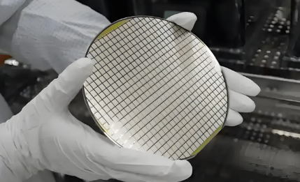
Physical design is the process of transforming logic design into an actual physical layout, with layout and routing being the key aspects. It is like building a city; not only must the locations of various areas be reasonably planned (layout), but the roads connecting these areas must also be designed (routing). If there are issues in layout and routing, the chip will be unable to operate normally, much like a city with chaotic traffic. Let us explore the challenges in physical design from the perspectives of design rule violations and issues with critical paths and power design. During the layout and routing process, strictly adhering to design rules (Design Rule Check, DRC) is fundamental to ensuring successful chip manufacturing. However, due to the complexity of design and human oversight, violations of design rules occur frequently. The critical path refers to the longest path of signal transmission delay within the chip, directly determining the chip’s maximum operating frequency. If the critical path is too long and the signal delay exceeds design requirements, it will lead to timing violations, preventing the chip from operating normally at the expected clock frequency. Additionally, the design of the power network and ground planes is crucial for the chip’s performance and stability. If the power network design is unreasonable and cannot provide stable and sufficient power to various parts of the chip, it will cause power noise, affecting the integrity of signals within the chip.
Timing analysis is a key step in ensuring that signals within the chip are transmitted and processed at the correct time, much like a conductor controlling the rhythm of a symphony; any deviation can lead to a chaotic “performance”. Issues such as unreasonable clock tree synthesis, excessive clock skew, and incorrect timing constraint settings can directly result in the chip not meeting speed requirements. Clock tree synthesis is the critical process of accurately transmitting clock signals from the source to various functional modules. If clock tree synthesis is unreasonable, such as improper placement and quantity of buffers, it will lead to delays and deviations in clock signal transmission. Within the chip, signal integrity issues are like hidden “killers” that constantly threaten the normal operation of the chip. Problems such as signal crosstalk, electromagnetic interference, and reflections act as “noise” and “obstacles” during signal transmission, causing logical errors and degrading signal quality. Signal crosstalk is the interference phenomenon caused by capacitive and inductive coupling between adjacent signal lines. In high-speed digital circuits, the rapid change of signals enhances the electromagnetic interaction between adjacent signal lines, making crosstalk issues particularly prominent. When a signal on one signal line changes, it induces noise signals on adjacent signal lines, affecting the accuracy of the target signal.
In the chip tape-out process, the testing and verification phase serves as the last line of defense for product quality, and its importance cannot be overstated. If this line of defense has vulnerabilities, even if the previous design and manufacturing stages appear perfect, the final outcome may still fail. Insufficient testing and verification mainly manifest in the lack of design for testability and inadequate test vector generation.
Design for Testability (DFT) is a design methodology that fully considers testing requirements during the chip design phase, aiming to improve the chip’s testability and testing efficiency. If testability design is not considered during the design phase and sufficient test points are not added, it will lead to low test coverage, making it impossible to detect potential defects. In complex chip designs, the internal logic is often very intricate, making signals difficult to observe and control directly. Without reasonable design for testability, testers cannot conduct comprehensive testing of the various modules and logic within the chip. Test vectors are sets of input signals used to test the chip’s functionality and performance; they are like “exam questions” for the chip, needing to cover various possible logical states and boundary conditions to ensure the chip operates normally under all circumstances. However, in actual testing, it is not uncommon for test vectors to fail to cover all logical states and boundary conditions, leading to some design errors not being detected in time, ultimately resulting in tape-out failure.
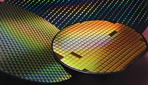
In the chip design process, Electronic Design Automation (EDA) tools are like a “magic wand” in the hands of designers, serving as a key support for achieving complex chip design and verification. However, these seemingly powerful tools hide many pitfalls, becoming potential factors leading to tape-out failures. Additionally, as the complexity of chip designs continues to increase, the accuracy requirements for simulation tools are also rising. In some advanced process chip designs, such as 5nm and 3nm technology nodes, device sizes have shrunk to the atomic level, and quantum effects begin to manifest. Traditional simulation tools based on classical physics models struggle to accurately simulate these quantum effects, thereby affecting the accuracy of performance predictions for the chip. This makes it difficult for designers to obtain sufficiently accurate simulation results to guide their designs, increasing the risk of tape-out failure. Layout checking is an important step to ensure that the chip layout meets manufacturing process requirements, and layout checking tools serve as the “gatekeepers” of this step. However, these tools are not flawless; they may fail to detect certain design rule violations, leading to tape-out failures.
In the chip tape-out process, team collaboration and communication are like tightly meshed gears; if any issues arise, the entire process can descend into chaos, becoming a potential factor for tape-out failure. Let us explore the impact of team collaboration issues on chip tape-out from the perspectives of communication barriers and chaotic version control. Chip design is a complex system engineering project involving multiple teams and professional fields, from front-end architecture design and logic design to back-end physical design and verification testing. Each stage requires close collaboration and precise communication between different teams. However, in actual projects, due to a lack of effective communication between teams, requirements are not accurately conveyed, and interface definitions are unclear, often leading to incorrect integration between modules, ultimately resulting in tape-out failure.
In the future, as semiconductor technology continues to develop, the integration of chips will become increasingly high, and the difficulty of design and manufacturing will continue to rise, presenting ever-greater challenges for tape-out. However, challenges coexist with opportunities, and new technologies and methods are constantly emerging, bringing hope for improving tape-out success rates. The application of technologies such as artificial intelligence and machine learning in chip design and verification is expected to enhance design efficiency and accuracy, allowing for timely detection of potential issues; at the same time, the continuous upgrading and improvement of EDA tools will provide stronger support for chip design. Furthermore, collaboration and communication within the industry will become closer, sharing experiences and resources to jointly tackle technical challenges and improve the overall tape-out success rate. We have reason to believe that with the joint efforts of all parties in the industry, the tape-out success rate will gradually improve, and the chip industry will usher in a more brilliant development.
For more details, please contact:

China’s well-known semiconductor agent and solution design provider
Dasheng Tang Electronics Co., Ltd.
(Shenzhen, Guangzhou, Beijing, Shanghai, Xi’an, Suzhou, Hong Kong)
Email: [email protected]
Website: www.szdst.com.cn

Long press to scan the code to follow
WeChat ID|DST-EIEC
|Dasheng Tang Electronics
1

Previous Highlights
Tianjin Semiconductor: Rising from the “Core” to Illuminate the Future
Unveiling the NPU: Unlocking the Secrets of Neural Network Processors
STMicroelectronics: Riding the Semiconductor Wave Amid Challenges
Chinese Memory Chips: Sailing Towards the Stars Amidst Breakthroughs and Reconstruction
Understanding CPU Virtualization: A Comprehensive Analysis from Principles to Pros and Cons
Milestones and New Journeys in China’s Chip Industry
Italian Semiconductors: The New Engine of Technology in an Ancient Country
Semiconductor Equipment: Current Status, Challenges, and Future
Xiaomi’s “Core” Power: Exploring the Secrets Behind Its Investment in Chip Companies
UCIE Bus: Breaking the Chiplet Interconnection Dilemma