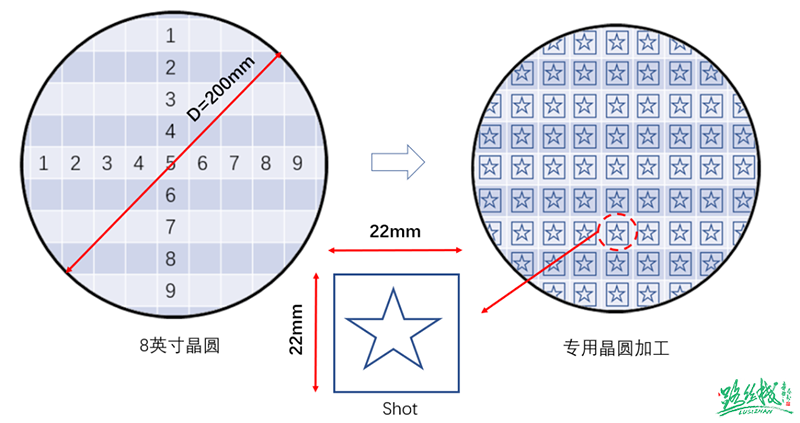
First, let’s explain what tape-out is; it is not the same as mass production. Tape-out, in English, is called Tape Out, is the process of converting a designed integrated circuit (IC) layout into an actual physical chip. It is like an assembly line, manufacturing chips through a series of process steps. Chip design companies hand over their designs to foundries for production.
The tape-out process is a key step in chip manufacturing, generally only a small number of samples are produced to check whether the chip meets design requirements or needs further optimization before deciding whether to proceed to mass production.
Chip Tape-Out Methods: Full Mask and MPW
Full Mask and MPW are both methods of tape-out for integrated circuits (handing over design results for production). Full Mask means that all masks in the manufacturing process serve a specific design; MPW stands for Multi Project Wafer, which translates to multiple projects sharing a wafer, meaning that multiple IC designs can be manufactured in a single production process.
1. Full Mask, meaning that all masks in the manufacturing process serve a specific design. With Full Mask chips, a single wafer can produce thousands of DIEs, which can then be packaged into chips, supporting large customer demand.
2. MPW, short for Multi Project Wafer, is similar to PCB panel prototypes, referred to as multi-project wafers. A multi-project wafer is where multiple integrated circuit designs using the same process are placed on the same wafer for tape-out. After manufacturing, each design can receive dozens of chip samples, which is sufficient for experiments and testing during the prototype design phase. This method can reduce tape-out costs by 90%-95%, significantly lowering the cost of chip development.
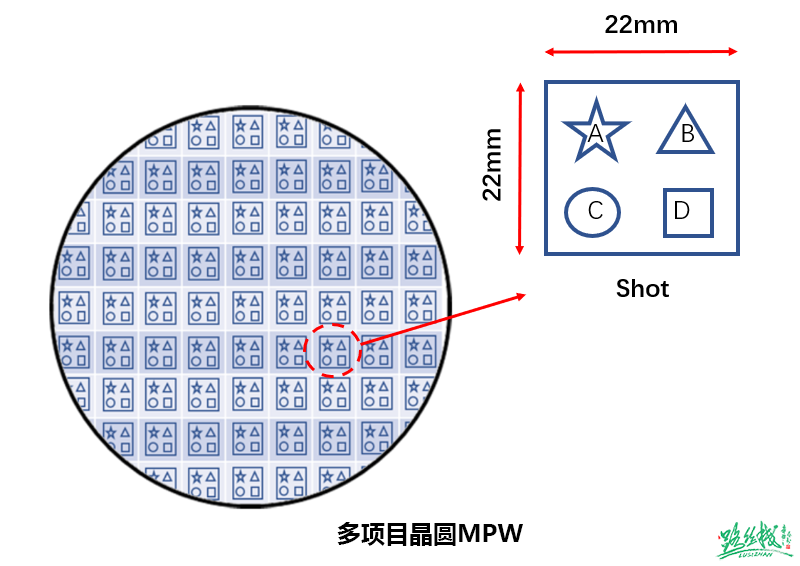 Foundries have fixed MPW opportunities every year, called Shuttle, which departs on schedule, quite a vivid analogy! Different companies share wafers, and there must be rules; MPW locks area by SEAT, generally a SEAT is an area of 3mm*4mm. Foundries usually limit the number of SEATs reserved for each company to ensure that different chip companies can participate in MPW (more SEATs would increase costs, negating the purpose of MPW). The advantage of MPW is the low tape-out cost, generally just a few hundred thousand, which significantly reduces risk. However, it is important to note that MPW is a complete production process from a manufacturing perspective, so it still takes time; an MPW typically requires 6 to 9 months, which delays chip delivery time.
Since it is a shared wafer, the number of chips obtained through MPW will be limited, mainly used for internal verification testing by chip companies, and may also be provided to a very small number of top customers. From this, it can be understood that MPW is an incomplete, non-mass-producible tape-out.
Why is chip tape-out so expensive?This brings us to the principles of chip manufacturing.
Foundries have fixed MPW opportunities every year, called Shuttle, which departs on schedule, quite a vivid analogy! Different companies share wafers, and there must be rules; MPW locks area by SEAT, generally a SEAT is an area of 3mm*4mm. Foundries usually limit the number of SEATs reserved for each company to ensure that different chip companies can participate in MPW (more SEATs would increase costs, negating the purpose of MPW). The advantage of MPW is the low tape-out cost, generally just a few hundred thousand, which significantly reduces risk. However, it is important to note that MPW is a complete production process from a manufacturing perspective, so it still takes time; an MPW typically requires 6 to 9 months, which delays chip delivery time.
Since it is a shared wafer, the number of chips obtained through MPW will be limited, mainly used for internal verification testing by chip companies, and may also be provided to a very small number of top customers. From this, it can be understood that MPW is an incomplete, non-mass-producible tape-out.
Why is chip tape-out so expensive?This brings us to the principles of chip manufacturing.
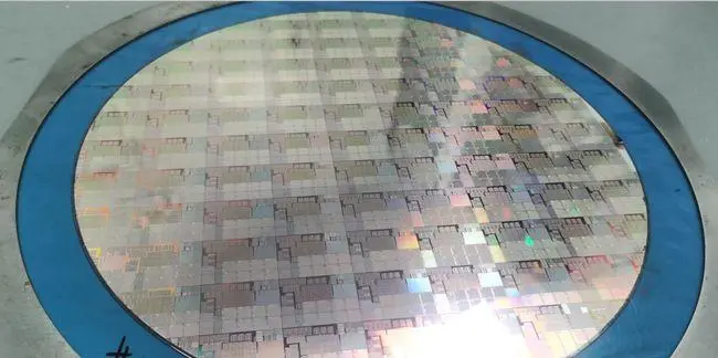
Chip manufacturing involves placing billions of transistors onto a very small chip, and the manufacturing process has reached the nanometer level, which can only be achieved through photolithography. Photolithography is the process of using light to project desired patterns, requiring the use of masks (also known as photomasks or Masks). The mask is where the designed circuit diagram is etched, allowing light to pass through and engrave the pattern on the wafer.
The high cost of tape-out is partly due to the many processes that need to be validated, from a circuit diagram to a chip, verifying whether each process step is feasible and whether the circuit has the required performance and functionality. The tape-out process typically lasts at least three months (including material preparation, photolithography, doping, electroplating, packaging, and testing), generally undergoing over 1000 processes, making it the most important and expensive step in chip manufacturing.
If the tape-out is successful, large-scale chip manufacturing can follow; otherwise, the reasons must be identified, and corresponding optimization designs must be made.
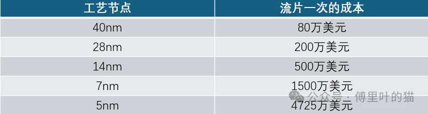
Of course, the cost of tape-out varies with different processes, and this is each company’s secret. However, there is a widely circulated data point suggesting that the differences are not very large among several process nodes encountered by some users.
From the image, the cost of tape-out masks at 40nm is approximately $800,000 to $900,000, and the wafer cost per piece is around $3,000 to $4,000. Including IP merge, it is unavoidable to run into several million RMB.For 28nm process tape-out, it costs $2 million per instance;For 14nm process tape-out, it costs $5 million per instance;For 7nm process tape-out, it costs $15 million per instance;For 5nm process tape-out, it costs $47.25 million per instance;For 3nm process tape-out, it may exceed $100 million!
Additionally, the high cost of chip tape-out is mainly attributed to masks and wafers, both of which are expensive and consumable. Among them, masks are the most expensive, with a set of mid-range process masks costing around $500,000, while a wafer costs several thousand dollars.
The more advanced the process node, the more layers of masks are required; each layer of “mask” corresponds to one application of photoresist, exposure, development, and etching, involving material costs and equipment depreciation costs, which all need to be borne by fabless customers!
For instance, 28nm requires about 40 layers, 14nm requires about 60 masks; 7nm requires 80 or even over a hundred masks; each mask costs $80,000, so chips must be mass-produced to lower costs!
Taking the 40nm MCU process as an example: If producing 10 wafers, the cost per wafer would be (900,000 + 4,000*10)/10 = $94,000; if producing 10,000 wafers, the cost per wafer would be (900,000 + 4,000*10,000)/10,000 = $4,090. (The larger the wafer quantity, the cheaper it gets; different manufacturers have different quotes.)
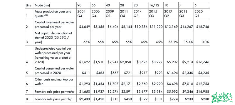
Wafer foundry prices, image source: Internet
Taiwan Semiconductor Manufacturing Company (TSMC) has provided the latest quote this year: for the most advanced 3nm process, the cost per wafer is $19,865, which is approximately 142,000 RMB.
Risks and Responses of Chip Tape-Out
Chip tape-out is still a high-risk endeavor; a chip development project requires going through a long process from product definition, design, verification, simulation to the final tape-out, and as the “ultimate exam,” any small oversight in the previous lengthy process could lead to tape-out failure! Achieving success in a single tape-out is often not easy.
For example, a certain analog chip company, even with a complete team and clear ideas, took 8 years and 18 tape-outs to finally complete the verification of sensor analog computing IP, creating the ideal ultra-low-power, ultra-near-field transmission chip.
Once tape-out fails, it often means the company faces losses starting from tens of millions of dollars and at least half a year of missed market opportunities, including financial losses, time waste, and project failures,leading to very serious consequences. Therefore, taking effective countermeasures is crucial.
Common countermeasures for tape-out failure include:
-
Strengthening Design Verification and Testing: Conducting thorough and rigorous simulation testing during the design phase, along with strict layout verification and timing analysis before actual tape-out, can help identify and rectify potential issues during the design phase, significantly improving the success rate of tape-out.
-
Tight Communication with Tape-Out Vendors: Various process and equipment issues may arise during the tape-out process. Establishing a regular communication mechanism with tape-out vendors to promptly feedback and resolve issues is crucial for ensuring the smooth progress of tape-out.
-
Establishing a Comprehensive Failure Analysis and Improvement Mechanism: Even with sufficient preventive and preparatory work, the possibility of tape-out failure still exists. By conducting an in-depth analysis of the reasons for failure, the root causes can be identified, and designs and tape-out processes can be optimized to prevent similar issues from occurring again.
Reducing the risks of tape-out failure requires a multi-faceted approach, including strengthening design verification and testing, maintaining close communication with tape-out vendors, and establishing a comprehensive failure analysis and improvement mechanism. Implementing these measures can not only improve the success rate of tape-out but also provide strong support for the sustainable development and technological innovation of the semiconductor manufacturing industry.
As the National Day holiday approaches, it is the best time for those busy with studies and work to enhance themselves! Whether you are a college student majoring in electronics or an engineer already in the chip design industry, our chip design training courses will give you a helping hand!
From September 26 to October 8, during the National Day holiday, E Course Network is offering very strong promotional activities for all IC courses on the entire site, helping you stand out in career competition!
National Day Promotion Courses Inquiry/Registration
E Course Network (www.eecourse.com) is a professional integrated circuit education platform under Moore Elite, dedicated to cultivating high-quality integrated circuit professionals in the semiconductor industry. The platform is oriented towards the job demands of integrated circuit companies, providing a training platform that aligns with the corporate environment, quickly cultivating students to meet corporate needs.
E Course Network has a mature training platform, a complete course system, and a strong faculty. It plans 168 high-quality courses in China’s semiconductor curriculum system, covering the entire integrated circuit industry chain, and has 4 offline training bases. To date, it has deeply trained a total of 15,367 people, directly supplying 4,476 professional talents to the industry. It has established deep cooperative relationships with 143 universities and has held 240 corporate-specific IC training sessions.