Often, we encounter the terms “tape-out” and “wafer” and many people mistakenly believe they refer to the same concept. In fact, the connotations and emphases of the two are completely different. In simple terms, tape-out is a process, while a wafer is a physical medium. Let’s break this down step by step.
1. Debunking Myths — The Wafer is the “Canvas”, Tape-out is the “Final Blueprint”
In the cornerstone of modern technology — the semiconductor industry, “tape-out” (流片) and “wafer” (晶圆) are two frequently used technical terms, but their meanings, roles, and essential differences are often confused. A precise understanding of these two concepts is key to insight into the complex ecosystem of chip design and manufacturing.
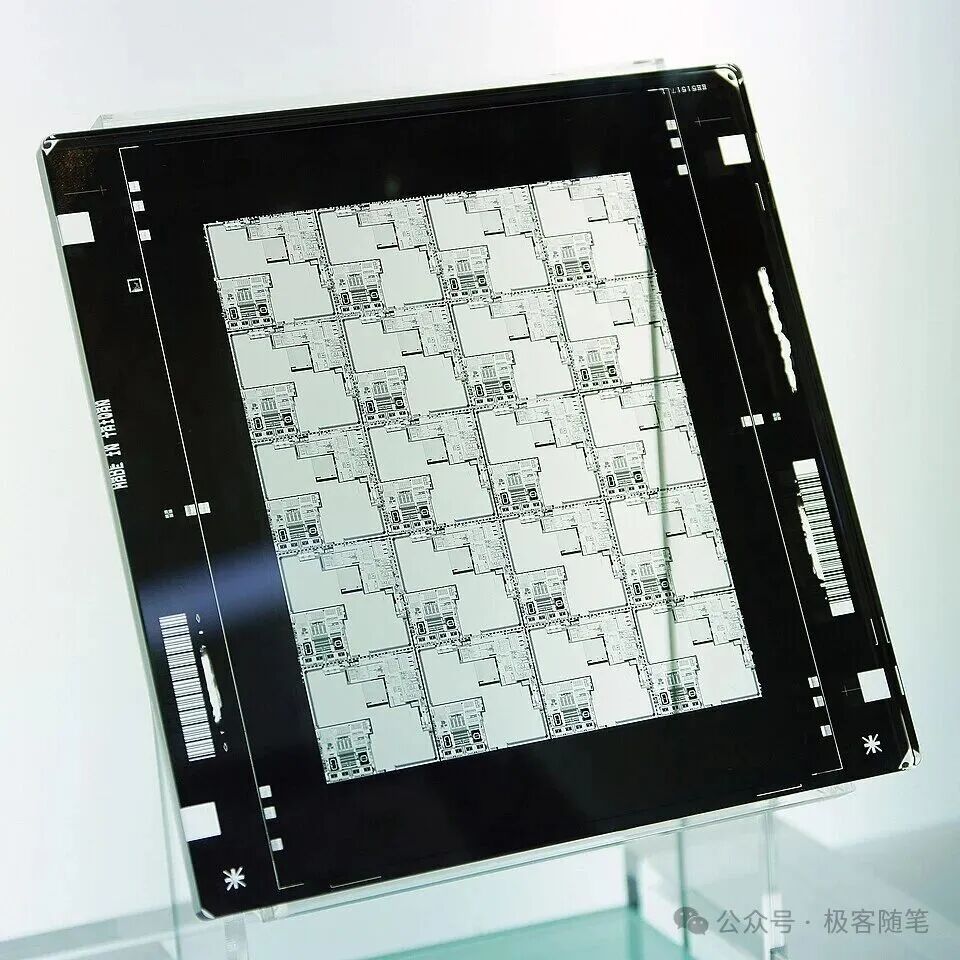
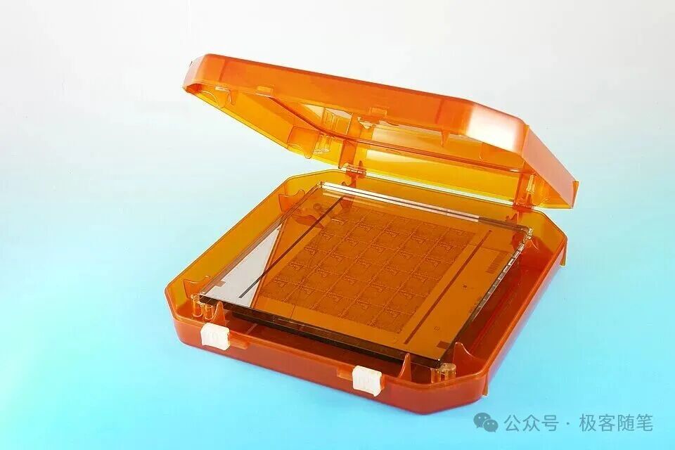
A wafer is a physical entity, serving as the “canvas” or “foundation” for chip circuits. It is a circular thin slice made from high-purity silicon material, formed through a series of precise processing steps, and serves as the physical medium for all subsequent manufacturing processes. In contrast, tape-out is a milestone or action in the design phase, representing the “final blueprint” of chip design. It signifies that the long and complex chip design work has been completed, and the design files can be delivered to the manufacturing plant to enter the actual production phase.
To better understand this relationship, we can use an analogy of building construction. In this analogy, the wafer is like the foundation and brick materials of a construction site. Without a solid wafer, no complex circuit can be attached. Tape-out, on the other hand, is akin to the final construction drawings submitted by an architectural firm. This drawing is the culmination of months or even years of design work, and once finalized, it means that the project can enter the formal construction phase. The key that connects these two is the photomask, which is like a precise mold or template made according to the construction drawings, accurately replicating every detail from the blueprint onto each brick.
2. The “Canvas” of Chips: The Birth and Physical Properties of Wafers
The wafer is the physical starting point of the semiconductor industry. Its birth is a magical journey that transforms the most common substance on Earth — sand, into a carrier of human wisdom. This process demands near-obsessive requirements for purity, precision, and materials science.
2.1 From Sand to Wafer
The raw material for wafers is silicon dioxide (SiO2) found in sand. These ores are first refined through an electric arc furnace and undergo a series of complex chemical treatments, including hydrochloric acid chlorination and distillation, ultimately being refined into polycrystalline silicon with a purity of up to 99.999999999%. This extremely high purity polycrystalline silicon is a prerequisite for producing electronic-grade silicon wafers.
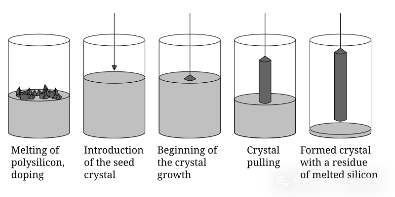
Next is the “crystal pulling” process. The purified polycrystalline silicon is melted into a liquid and then slowly pulled into large single crystal silicon ingots using methods like the Czochralski process. This step is crucial as it ensures the atomic arrangement of the silicon material is uniform, forming a perfect single crystal structure, laying the physical foundation for manufacturing micro-nano sized transistors on the wafer.
Subsequently, the large single crystal silicon ingot is cut into thin slices of a certain thickness using precision tools (such as diamond saws), and these slices are what we refer to as “wafers”. To achieve a nanometer-level flatness on the wafer surface, suitable for subsequent high-precision processes like extreme ultraviolet (EUV) lithography, the wafers must undergo multiple grinding, polishing, and cleaning steps. Ultimately, these processed silicon slices become the basic raw material for integrated circuit factories, known as “wafers”.
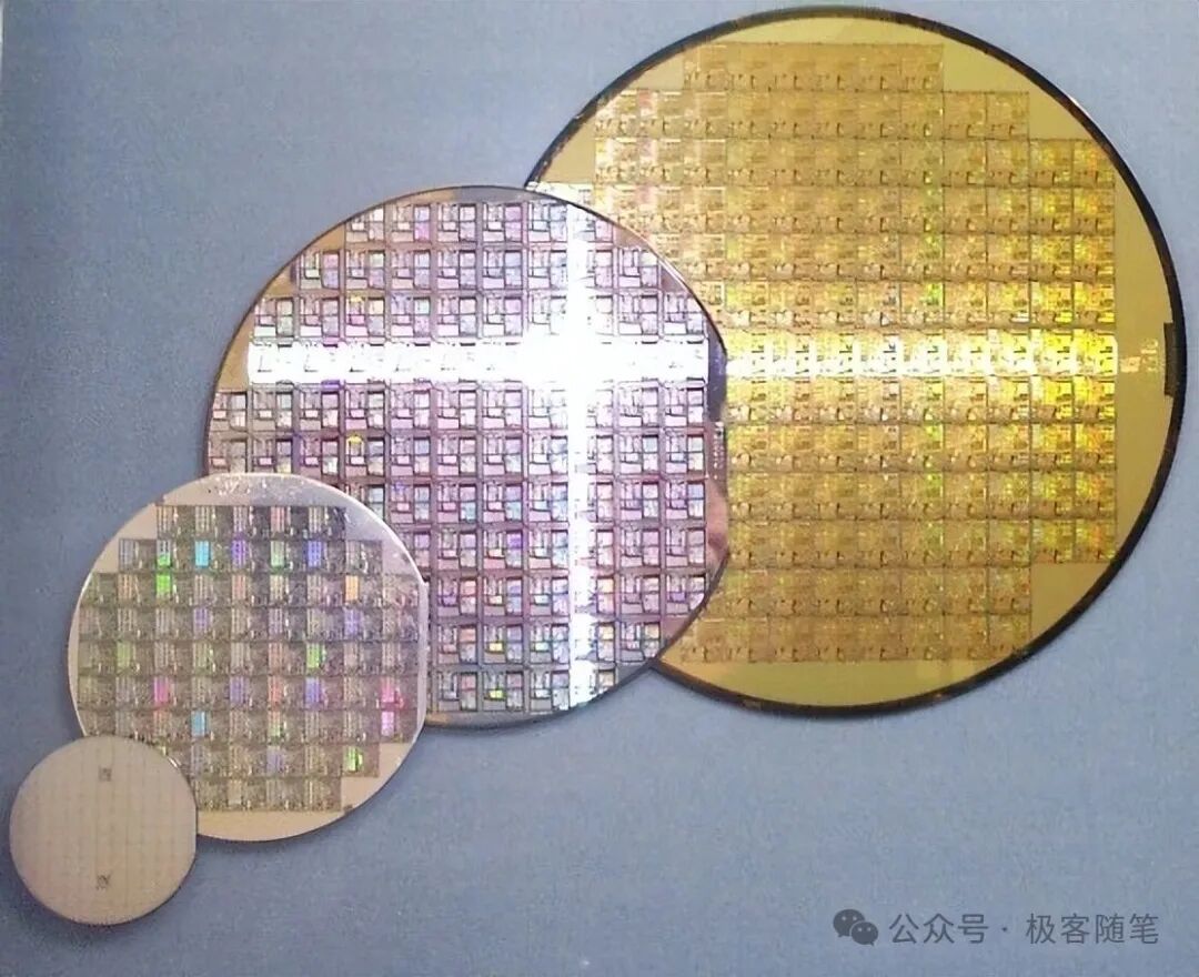
2.2 The “ID Card” of Wafers: Size and Material
The size of a wafer is a key indicator of the semiconductor manufacturing technology level and industrial economic efficiency. The evolution of wafer diameter (from 6 inches, 8 inches to 12 inches/300mm) is actually a profound economic transformation. This is not just a technological advancement but also a strategic choice driven by economies of scale.
One of the core goals of semiconductor manufacturing is to improve production yield and reduce unit costs. The area of a wafer increases proportionally with the square of the radius (Area = πr²), while the wasted area at the wafer edge, known as the “wafer edge effect”, increases linearly (Perimeter = 2πr). As the diameter of the wafer increases, its total area significantly increases, while the proportion of unusable edge area decreases. This directly leads to a substantial increase in the number of chips that can be produced from a single wafer, significantly diluting the manufacturing cost per chip. This scaling effect significantly enhances the profitability and market competitiveness of wafer foundries. This also explains why industry giants like Intel, TSMC, and Samsung have been actively exploring the research and commercialization of 450mm wafers, despite facing numerous technical challenges.
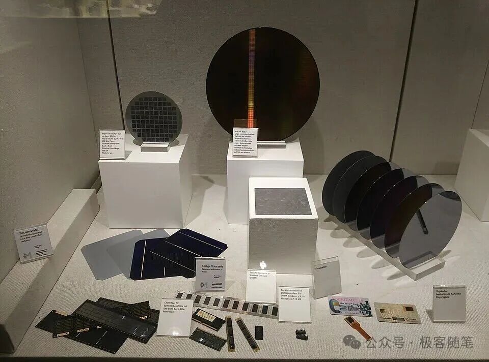
Moreover, the materials for wafers are also diversifying to meet the demands of specific application markets. In addition to mainstream silicon (Si) wafers, wide bandgap semiconductor materials like gallium nitride (GaN) and silicon carbide (SiC) wafers have emerged. This diversification of materials reflects the specialization and segmentation of semiconductor technology. As the physical limits of silicon-based devices are reached in certain high-power, high-frequency applications (such as electric vehicles and 5G base stations), the market seeks new materials with higher bandgap widths, better thermal conductivity, and high-temperature resistance. Therefore, GaN and SiC wafers are used to manufacture power semiconductors and RF devices, which have their own independent R&D and mass production timelines, forming a highly specialized wafer manufacturing ecosystem parallel to traditional silicon wafer manufacturing. This indicates that “wafer” is not a single concept but is highly segmented based on its materials and application fields.
3. The “Blueprint” of Chips: The Definition and Milestone Significance of Tape-out
If the wafer is the “canvas” of the physical world, then tape-out is the “instruction” that transitions from the abstract design world to the physical world. Tape-out is an action of significant symbolic meaning, rather than a physical entity.
3.1 What is Tape-out? Definition, Action, and Symbolic Significance
Tape-out (流片), also known as “off-line” or “design finalization”, is the last step in the design of integrated circuits (IC) or printed circuit boards (PCB). This term originates from early integrated circuit design when designers needed to draw circuit layout diagrams on large “tape” and then deliver the tape to the manufacturing plant. Today, this process has become highly digitalized, but the term “tape-out” has been retained, and its core meaning remains unchanged: submitting the designed circuit diagram to the wafer foundry for production.
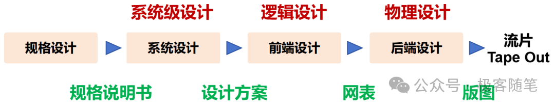
Therefore, tape-out is a “delivery action” from “design” to “manufacturing”. In the semiconductor industry, it is not just a technical step but also an important milestone, marking the completion of months or even years of design, simulation, and verification work, allowing the design team to celebrate this phase victory. For example, the self-developed chip Xuanjie O1 uses advanced 3nm process technology, and the cost of a single tape-out exceeds $20 million. It sends a clear signal to the outside world: the design work for this chip is complete and can enter actual production.
3.2 The “Product” of Tape-out: Photomask — The Physical Bridge Connecting Design and Manufacturing
The final result of the tape-out phase is a set of design files used to create photomasks, typically in GDSII format. The photomask is the physical key to understanding the relationship between tape-out and wafers, as it transforms the abstract digital design represented by tape-out into a physical “template” that can be recognized and projected by lithography machines.
The photomask is the “mold” required for producing integrated circuits, essentially a glass or quartz plate with an opaque pattern. During the lithography process, it acts like a negative in photo development, accurately projecting the circuit pattern onto the wafer.
The photomask carries all the design information from the tape-out, and the patterns on it are reduced by 4 to 10 times (modern lithography machines typically by 4 times) and accurately projected onto the wafer surface. The wafer foundry then uses this photomask to perform multi-layer lithography on the wafer, transforming the design blueprint into physical circuit structures. Therefore, the precision of the photomask directly determines the quality and yield of the final chip.
4. From Blueprint to Canvas: The Journey of Integration Between Tape-out and Wafer
After understanding the fundamental differences between tape-out and wafers, we can examine them within the macro process of chip manufacturing. The birth of a chip can be divided into three core stages: chip design (ending with “tape-out”), wafer manufacturing (the physical process after tape-out), and packaging and testing. Tape-out is the critical node that connects the two, serving as the “endpoint” for the design team and the “starting point” for the manufacturing team.
4.1 A Macro View of Chip Manufacturing
During the chip design phase, designers use specialized electronic design automation (EDA) tools to create circuit diagrams and layouts based on application requirements. Once the design scheme has undergone repeated simulations and verifications and is confirmed to be correct, tape-out is completed, and the design files are submitted to the wafer foundry.
After the tape-out action is completed, the chip design blueprint is gradually realized on the wafer “canvas” step by step. This process is the core embodiment of the integration of tape-out and wafers and is the most complex and precise part of chip manufacturing. It involves thousands of processes and typically takes several weeks to complete.
4.2 Analysis of the Manufacturing Process After Tape-out
After the tape-out action is completed, the wafer foundry will initiate a series of precise manufacturing processes to transform the blueprint into physical circuits:
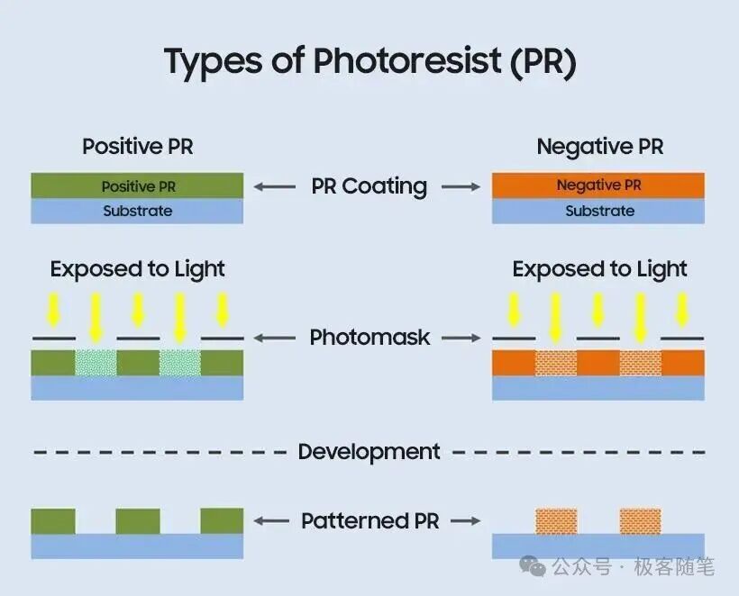
Lithography and Etching: This is the core of the entire manufacturing process. The wafer surface is first coated with a layer of photoresist. The lithography machine projects the circuit pattern onto the photoresist through the photomask, causing a chemical reaction in the exposed areas.
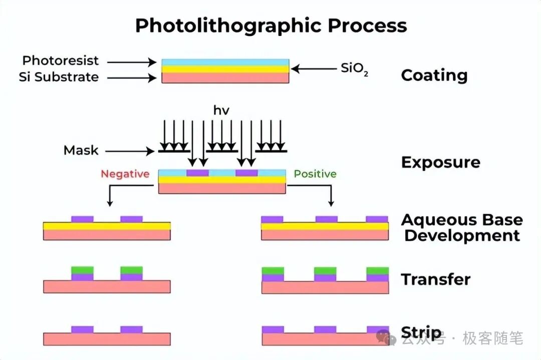
Then, the unexposed parts of the photoresist are removed using a developer, exposing specific areas of the wafer surface. Finally, chemical solutions or plasma are used to etch the exposed areas, forming the circuit structures.
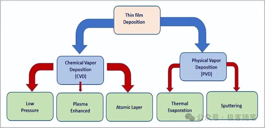
Thin Film Deposition: Using methods such as chemical vapor deposition (CVD) or physical vapor deposition (PVD), one or more layers of thin films, such as metals, oxides, or nitrides, are deposited on the wafer surface. These films are used to form structures like wires and insulating layers in the circuit.
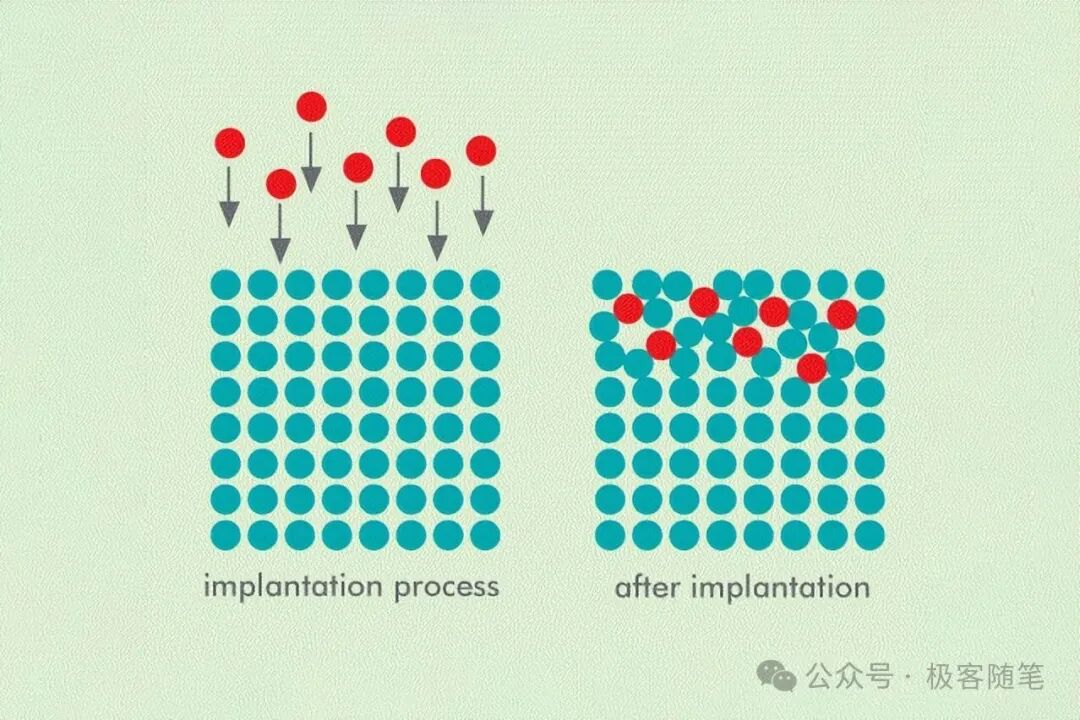
Ion Implantation: Specific types of ions, such as boron and phosphorus, are implanted into specific areas of the wafer surface using an ion implanter. This process aims to alter the conductivity of these areas, forming key structures like the PN junctions of transistors.
Annealing and Cleaning: The wafer undergoes annealing treatment in a high-temperature environment to relieve stress, improve electrical performance, and promote ion diffusion within the wafer. At the same time, high-purity chemical solutions are used to clean the wafer, removing residual impurities and contaminants from the surface.
All these complex processes occur on the same wafer, layer upon layer, ultimately forming a complete integrated circuit.
4.3 Core Differences and Collaborative Relationships
To better understand the roles, positions, and attribute differences of tape-out and wafers in the chip production chain, we can use the following table for a visual comparison.
Core Differences Between Tape-out and Wafer
|
Characteristic |
Tape-out |
Wafer |
|
Essence |
Milestone or action in the design phase |
Physical material in the manufacturing phase |
|
Role |
Finalization of chip design, the “blueprint” |
Carrier of chip circuits, the “canvas” |
|
When it Occurs |
Before wafer manufacturing, signaling its start |
The entire wafer manufacturing process, the carrier of all processes |
|
Main Costs |
Labor costs for chip design, EDA tool costs, photomask production costs |
Silicon material purification costs, wafer manufacturing equipment (such as lithography machines) costs, factory operating costs |
|
Core Output |
Design files for photomasks (e.g., GDSII) |
Silicon slices carrying chip circuits |
5. Why is the Distinction Between Tape-out and Wafer So Important?
The precise distinction between tape-out and wafers is not just a technical conceptual clarification; it profoundly reveals the economic structure and operational model of the modern semiconductor industry.
5.1 Economic Perspective: High Risk and High Investment Decision Points
Tape-out is a high-risk decision in the chip R&D process. As semiconductor process nodes (such as 5nm, 3nm) continue to advance, the sizes of transistors within chips are becoming smaller and their densities higher. This exponentially increases the precision requirements for photomasks. The photomask production process for advanced technologies is more complex, and costs have risen accordingly, with the cost of a single photomask potentially reaching millions or even tens of millions of dollars. For instance, Xiaomi’s 3nm Xuanjie O1 has a tape-out cost exceeding $20 million.
This cost structure makes each tape-out a significant financial commitment. If defects are found in the design after tape-out, requiring design modifications and a re-tape-out, known as a “respin”, the costs can be enormous, potentially leading to the failure of the entire project. This highlights the strategic importance of the tape-out action, as it is a major financial commitment and a critical node determining the project’s success.
5.2 Industry Ecology: The Division of Labor Between Fabless and Foundry
The concepts of tape-out and wafer naturally delineate the two mainstream business models in the modern semiconductor industry:
- Fabless Companies: These companies focus on chip design, with their core work being the completion of “tape-out”. They do not own or operate expensive wafer manufacturing plants. For example, companies like Qualcomm and NVIDIA have design teams responsible for transforming ideas into tape-out files, which are then submitted to wafer foundries for production. The tape-out news of NVIDIA’s Rubin chip is a core outcome of its work as a fabless company.
- Foundries: These companies specialize in wafer manufacturing, with their core assets being advanced wafer production lines and top-notch manufacturing technologies. They receive tape-out files (photomasks) from fabless companies for manufacturing, such as TSMC and SMIC.
This division of labor is key to the rapid development and innovation of the semiconductor industry. If a company both designs and manufactures (i.e., a vertically integrated manufacturer, IDM model, like Intel), the financial pressure is immense, and it is difficult to maintain leadership in both areas. Separating design from manufacturing has allowed fabless companies to focus on innovation while foundries concentrate on processes, significantly lowering the barriers to chip design and stimulating design innovation globally, while ensuring continuous progress in wafer manufacturing technology.
6. Conclusion
In summary, tape-out and wafers are two distinctly different yet interdependent core concepts in the chip birth process. The wafer is the physical medium, the “stage” for all manufacturing processes; while tape-out is the design finalization, the “instruction” to commence manufacturing. Together, they form the foundation of modern information society.
The precise distinction between the two concepts not only helps us understand the complex processes of chip manufacturing but also profoundly reveals the economic necessity of specialization in the modern semiconductor industry. Wafer foundries focus on the limits of physical manufacturing, while fabless companies concentrate on the infinite creativity of the digital world. This separation of “design” and “manufacturing” greatly lowers the barriers to innovation and accelerates technological iteration.
Semiconductor technology will continue to advance towards smaller process nodes while exploring the applications of new wafer materials (such as GaN and SiC) in specific fields. Additionally, the industry’s pursuit of larger wafer sizes will continue to enhance production efficiency and reduce costs. These trends will deepen the connotations of both tape-out and wafers and drive the entire industry forward, creating a smarter and more interconnected future for humanity.