
-
Photolithography Machine: As the core equipment in the fabrication process, its accuracy and stability have a decisive impact on the quality of the chip pattern transfer. Modern photolithography machines use advanced optical systems and precise mechanical structures to project layout patterns onto silicon wafers with extremely high resolution, thereby achieving precise delineation of fine patterns. Photolithography machines are also equipped with advanced alignment systems to ensure that each exposure aligns accurately with existing patterns on the silicon wafer, ensuring the accuracy and consistency of the chip structure. -
Etching Equipment: During the fabrication process, etching equipment removes specific materials from the surface of the silicon wafer through chemical or physical methods, forming the required grooves, holes, or microstructures. The performance of etching equipment directly affects the dimensional accuracy and surface roughness of the chip, thereby impacting the electrical performance and reliability of the chip. When selecting etching equipment, it is essential to consider factors such as etching rate, selectivity, uniformity, and the extent of damage to the silicon wafer surface. -
Deposition Equipment: This is the key equipment used to deposit various thin film materials on the surface of the silicon wafer. These thin film materials include metals, oxides, nitrides, etc., which play an important role in constructing the internal structure of the chip and achieving specific functions. The performance of deposition equipment directly affects the composition, structure, thickness, and uniformity of the thin film materials, thereby influencing the performance and stability of the chip. When selecting deposition equipment, factors such as deposition rate, composition control, thickness uniformity, and process stability need to be considered.
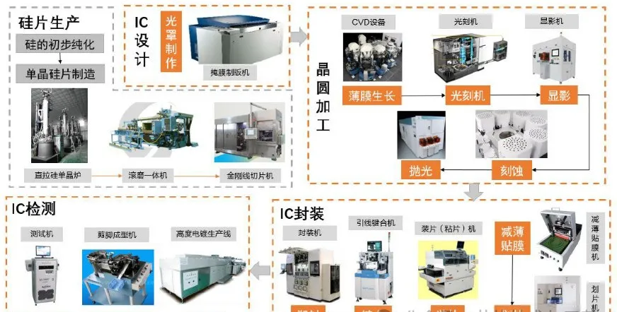
Material selection and usage are crucial stages in the chip fabrication process.
-
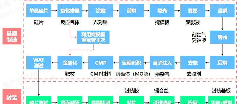
Photoresist: As one of the core materials in chip manufacturing, its performance directly relates to the accuracy and resolution of pattern transfer. High-quality photoresist should have good photosensitivity, adhesion, and corrosion resistance to ensure that the desired pattern mask can be accurately formed during the photolithography process. Additionally, the removal of photoresist must also be precisely controlled to avoid damaging the silicon wafer surface or leaving residues. -
Etching Gases: Play a key role in removing excess material and forming fine structures during chip fabrication. Different etching gases have selectivity for different materials, so it is essential to choose the appropriate etching gases based on actual needs. Furthermore, parameters such as temperature, pressure, and time during the etching process must also be precisely controlled to ensure uniformity and accuracy of the etching. -
Thin Film Materials: Play an important role in constructing the internal circuits and interconnect structures of the chip. The deposition of thin film materials such as metals and oxides requires precise control of parameters like thickness, uniformity, and purity to ensure the stability of circuit connections and signal transmission within the chip. Additionally, the properties and stability of thin film materials directly affect the reliability and lifespan of the chip.
|
|
|
|
|
|
|
|
|
|
|
|
|
|
|
|
|
|
|
|
|
|
|
|
|
|
|
|
|
|
|
|
|
|
|
|
|
|
|
|
|
|
|
|
|
|
|
|
|
|
|
|
|
|
|
|
|
|
||
|
|
|
|
||
|
|
|
|
||
|
|
|
|
-
Design Complexity: The increase in the length and density of interconnections also makes design and verification more complex. -
Advances in Process Technology: High precision requirements have driven the technological leap from deep submicron to nanoscale processes. This imposes higher demands on equipment accuracy and material performance, leading to increased equipment costs and difficulties in material research, development, and procurement. At the same time, high-precision processes require stricter quality control to ensure the stability and reliability of each production stage, further increasing the overall cost of fabrication. -
Countermeasures:
-
Design Phase: Introduce more efficient design tools and methods, such as high-level synthesis and automated routing, to improve design efficiency and reduce human errors. Use hierarchical and modular design concepts to decompose complex systems into more manageable submodules, thus reducing design complexity.
-
Cost Control: Optimizing process parameters and material selection is key. In-depth research on process principles and material performance to find more cost-effective process schemes and material combinations. Increasing equipment utilization and reducing waste rates are also effective ways to lower costs. Strengthening communication and collaboration with supply chain partners ensures the stability and reasonable pricing of material supplies.
-
Strengthen Design Verification and Testing: Conduct detailed and rigorous simulation testing during the design phase, as well as strict layout verification and timing analysis before actual fabrication, to identify and correct potential issues as early as possible, significantly improving the success rate of fabrication. -
Close Communication with Fabrication Vendors: Various process and equipment issues may arise during fabrication; establishing a regular communication mechanism with fabrication vendors to promptly feedback and resolve issues is crucial to ensuring smooth fabrication. -
Establish a Comprehensive Failure Analysis and Improvement Mechanism: Even with thorough preventive measures in place, the possibility of fabrication failures still exists. Through in-depth analysis of failure causes, the root of the problem can be identified, and design and fabrication processes can be optimized to prevent similar issues from recurring.

Wuxi Qixin Semiconductor Technology Co., Ltd. is a high-tech enterprise specializing in the research, development, production, and sales of intelligent manufacturing equipment for the chip industry. Founded in 2020, it is located in the Wuxi Huishan Economic and Technological Development Zone. The company has received multiple honors such as Wuxi Huishan District Pioneer Talent and Wuxi Taihu Talent, and is a council member of the Wuxi Semiconductor Association. The core members of the company’s R&D team have over 20 years of experience in semiconductor equipment, with rich R&D experience in packaging processes and related equipment industrialization, holding multiple national-level technology invention and utility model patents as well as software copyrights. The company has long-term partnerships with well-known domestic institutions such as Tsinghua University and the Chinese Academy of Sciences for industry-university-research collaborations.
The MGP intelligent chip packaging system, AM fully automatic chip packaging system, and TF unit modular chip automatic cutting and forming system, all developed independently by Wuxi Qixin Semiconductor Technology Co., Ltd., have been recognized by the market and received unanimous praise from customers.
Wuxi Qixin Semiconductor Technology Co., Ltd. adheres to the values of innovation, efficiency, quality, and integrity, based in Wuxi, with the mission of creating Chinese independent brand chip intelligent equipment, assisting the chip industry, and building smart factories. It aims to become a leader in the chip packaging and testing equipment industry!