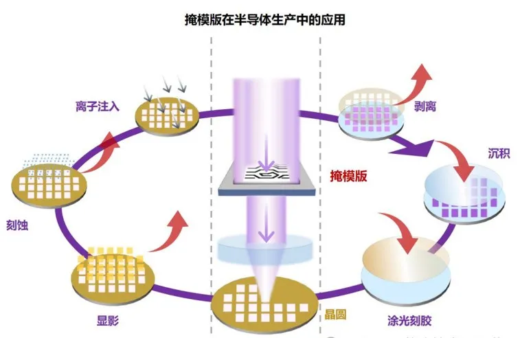
Detailed Explanation of Chip Tape-Out Technology
3.1 Design Check and Layout Verification
Before proceeding with chip tape-out, design checks and layout verification are essential steps that are crucial for ensuring the success of the tape-out.
-
Design Rule Check (DRC):The main purpose of this process is to thoroughly review the chip layout to confirm that it strictly adheres to manufacturing process rules. This includes checks on key parameters such as line width, spacing, and layering. Using high-precision software tools, the layout can be automatically scanned to identify any design elements that may violate manufacturing process rules. Once violations are detected, the design team receives immediate feedback for adjustments. This preventive check mechanism significantly improves the yield of chip manufacturing and reduces production risks caused by design errors.
-
Layout Verification (LVS):This step ensures a high degree of consistency between the chip layout and the original circuit design. Verification tools compare the schematic and layout, checking each component and connection to ensure that the layout accurately reflects the intent of the circuit design, guaranteeing that functionality and performance meet expected standards.
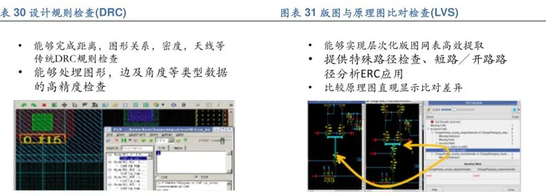
Design checks and layout verification are not one-time tasks. During the design and tape-out process, these two steps may iterate multiple times to ensure continuous improvement and optimization of the design, with each modification passing through strict verification processes. This iterative verification approach enhances design reliability and lays a solid foundation for subsequent chip testing and mass production.
3.2 Layout Routing and Mask Production
As the core aspect of chip design, layout routing is inherently complex.In this process, designers need to meticulously plan each line to ensure that it meets functional requirements while achieving optimal performance metrics.
-
Signal Integrity:One of the critical factors to consider during routing, which relates to whether the chip can stably and accurately transmit signals during actual operation.
-
Timing Issues:Reasonable timing design ensures that the chip does not encounter timing confusion or signal delay issues during high-speed operation.
-
Power Consumption Control:An increasingly important aspect in modern chip design; effective power management can not only improve the chip’s energy efficiency but also extend its lifespan.
|
|
|
|
|
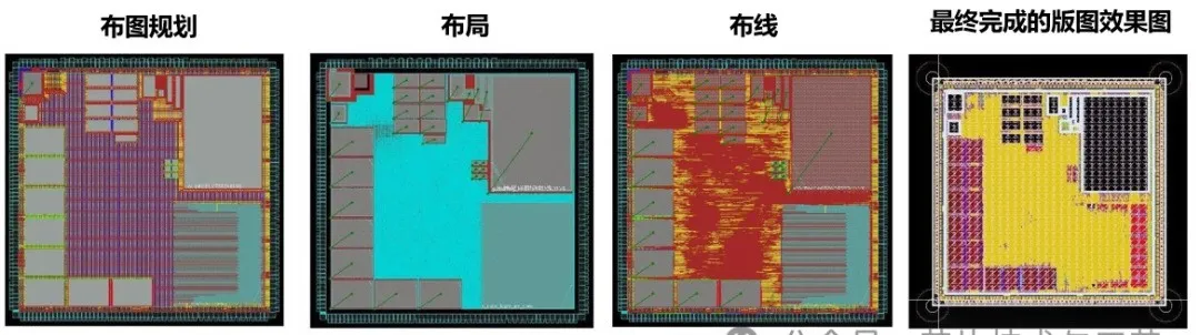
Completion Effect of Layout Planning
|
The outermost circle is I0PAD, which is the interface connecting the chip to the outside. The large gray and green modules in the figure are the main IPs.
The red and blue lines in the figure are power stripes, used to connect the power and ground signals of various components and modules throughout the chip, and are generally wider.
|
Layout planning is a crucial step in the entire backend process, but it is also the most flexible step. There is no standard optimal solution, yet many details need to be considered. The goal of layout routing: optimize the chip area, timing convergence, stability, and ease of routing.
|
|
Completion Effect of Layout
|
The gray and green parts in the figure are the main IPs.
The remaining blue parts are standard cells, filled automatically by the software. The software will automatically leave appropriate space for the next step of routing.
|
Layout involves placing standard cells, I/O pads, and macro cells to realize the logic of the circuit.
The layout goal: the higher the utilization, the better; the shorter the bus length, the better; the faster the timing, the better.
However, the higher the utilization, the more difficult the routing becomes; the longer the bus length, the slower the timing. Therefore, a balance among these three parameters must be achieved.
|
|
Completion Effect of Routing
|
The red and yellow metal lines are automatically routed on the standard cells by the software.
|
Routing refers to connecting various units and I/O pads with interconnect lines while satisfying the constraints of process rules, routing layer limits, line width, line spacing, and ensuring the electrical performance constraints of reliable insulation between lines.
|
|
|
Compared to before, the layout and routing of some areas have been redone to meet timing requirements and DRC, LVS requirements. “Filler” has been added to meet the design rule regarding metal layer density requirements.
|
Clock Tree Synthesis, simply put, is the routing of the clock. Since the clock signal plays a global commanding role in digital chips, its distribution should be symmetrical to each register unit, thereby minimizing the clock delay differences from the same clock source to each register. This is why clock signals need to be routed separately.
LVS (Layout Vs Schematic) verification: simply put, it is the comparison verification between the layout and the gate-level circuit diagram after logic synthesis;
DRC (Design Rule Checking): checks whether the line spacing, line width, etc., meet process requirements;
ERC (Electrical Rule Checking): checks for electrical rule violations such as short circuits and open circuits; the actual backend process also includes circuit power consumption analysis and DFM (Design for Manufacturability) issues arising with the continuous advancement of manufacturing processes, etc.
The physical layout is delivered to the chip foundry in GDSII file format to create the actual circuit on silicon wafers.
|
After completing the layout routing, the subsequent mask production stage is equally crucial.
|
|
|
|
|
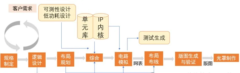
Defines the detailed specifications of the chip’s functions, performance, interfaces, and power requirements, providing guidance for subsequent design work.
|
|
Design for Testability (DFT)
|
Considers the testability of the circuit during the design phase to facilitate effective defect detection and diagnosis after manufacturing.
|
|
Design for Low Power (DLP)
|
Adopts specific techniques during the design phase to reduce the chip’s power consumption to meet energy-saving or battery life requirements.
|
|
Dynamic Test Vector Generation
|
Generates dynamic test vectors for testing the chip after manufacturing, which will be used during the actual testing phase.
|
|
|
Defines the detailed specifications of the chip’s functions, performance, interfaces, and power requirements, providing guidance for subsequent design work.
|
|
|
Provides the basic building blocks and pre-designed, reusable design components needed for chip design.
|
|
|
Uses hardware description language (HDL) to write code to implement the functional logic of the chip.
|
|
|
Determines the positions and sizes of various modules on the chip and their interconnections, laying the foundation for layout routing.
|
|
|
Converts HDL code into a gate-level netlist, which is the process of transforming abstract hardware descriptions into concrete circuit representations. The gate-level netlist details the logic gates and their connections in the circuit, providing input for physical design and timing analysis.
|
|
|
Uses simulation tools to verify whether the circuit’s functions and performance meet expectations.
|
|
|
Converts the gate-level netlist into an actual physical layout and completes the routing, ensuring correct signal connections on the chip.
|
|
Mask Generation & Verification
|
Generates the mask patterns used for manufacturing the chip and verifies that the layout is consistent with the design specifications.
|
|
|
Produces masks based on the verified layout. These masks will be used in the subsequent chip manufacturing process for pattern transfer.
|
The mask, as the bridge for transferring the design pattern from the virtual world to the real silicon wafer, has its production accuracy directly impacting the final quality of the chip.
|
Downstream Application MarketField
|
|
Product Application Field
|
Downstream Application Representative Manufacturers
|
|
|
|
Logic circuit manufacturing, analog circuit manufacturing, power device manufacturing, MEMS sensor manufacturing, IC packaging, etc.
|
Semi-conductor manufacturing industry
|
Taiwan Semiconductor Manufacturing Company, Intel, SMIC, Hua Hong Semiconductor, China Resources Micro, SMIC Integration, Silan Microelectronics, JCET, BYD Semiconductor, Li’an Micro, Yandong Micro, Gaode Infrared, Changdian Technology, etc.
|
|
|
|
LCD screen manufacturing, OLED screen manufacturing, etc.
|
Display technology industry
|
BOE Technology Group, Tianma Microelectronics, Huaxing Optoelectronics, China Electronics Panda, Huike, etc.
|
|
|
PCB (Printed Circuit Board, Flexible Circuit) manufacturing, touch screen manufacturing, optical device manufacturing, etc.
|
PCB manufacturing, touch screen manufacturing, optical device manufacturing, etc.
|
Electronic manufacturing industry
|
Lens Technology, Zhi Xiang Electronics, etc.
|
|
Photolithography technology plays a key role in this stage, utilizing the principles of diffraction and interference of light to accurately project fine patterns from the layout onto the silicon wafer. Subsequently, through etching and other process steps, these patterns are transformed into actual physical structures, thus completing the chip production.
-
Increased Routing Density and Complexity:As the integration level of chips continues to rise, it poses significant challenges for designers.
-
Higher Precision and Efficiency Requirements for Mask Production:With the market’s increasing performance demands for chips, mask production faces higher requirements.
In summary, layout routing and mask production are indispensable parts of the chip tape-out process, and their technical level and implementation effectiveness directly relate to the final performance and quality of the chip.
Wuxi Qixin Semiconductor Technology Co., Ltd. is a high-tech enterprise specializing in the research, development, production, and sales of intelligent production equipment for the chip industry. Founded in 2020, it is located in the Huishan Economic and Technological Development Zone in Wuxi. The company has received multiple honors such as Wuxi Huishan Pioneer Talent and Wuxi Taihu Talent, and is a council member of the Wuxi Semiconductor Association. The core members of the company’s R&D team all have over 20 years of experience in semiconductor equipment, possessing rich R&D experience in packaging processes and related equipment industrialization, and hold multiple national-level technology invention, utility model patents, and software copyrights. The company has long engaged in industry-university-research cooperation with well-known domestic institutions such as Tsinghua University and the Chinese Academy of Sciences.
The self-developed MGP intelligent chip packaging system, AM fully automatic chip packaging system, TF unit modular chip automatic cutting and forming system, and other intelligent production equipment for chips have all received market recognition and unanimous praise from customers.
Wuxi Qixin Semiconductor Technology Co., Ltd. adheres to the values of innovation, efficiency, quality, and integrity, based in Wuxi, with the mission of creating intelligent equipment for Chinese independent brands of chips, supporting the chip industry, and building smart factories. It aims to become a leader in the chip packaging and testing equipment industry!
Disclaimer: This article is a network reprint or adaptation, and the copyright belongs to the original author. However, due to the numerous reprints, it is impossible to confirm the true original author, so the source of reprint is indicated. If there are any copyright issues, please contact us for deletion! The content of this article represents the views of the original author and does not represent the views of this public account or its responsibility for authenticity.