May.
Click the blue text to follow us
2025.05
 Comment at the end to win a popular ergonomic lumbar support chair!
In the rapid iteration of smart electric vehicles, the BYD Yangwang series, as a high-end flagship model of Chinese new energy vehicles, represents the pinnacle of domestic automotive electronic design with its ADAS hardware platform. In this issue, we will dissect the intelligent controller of the BYD Yangwang series, analyzing its chip selection and circuit design/layout to glimpse BYD’s core technology layout in the field of autonomous driving.
More exciting disassemblies
Please click to follow and star Eefocus
Disassembly
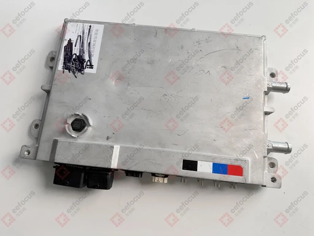
The BYD Yangwang ADAS board is quite heavy and difficult to disassemble, with densely packed internal chips, and the thermal grease on the casing is also quite extravagant (the specific disassembly process can be viewed in the video).
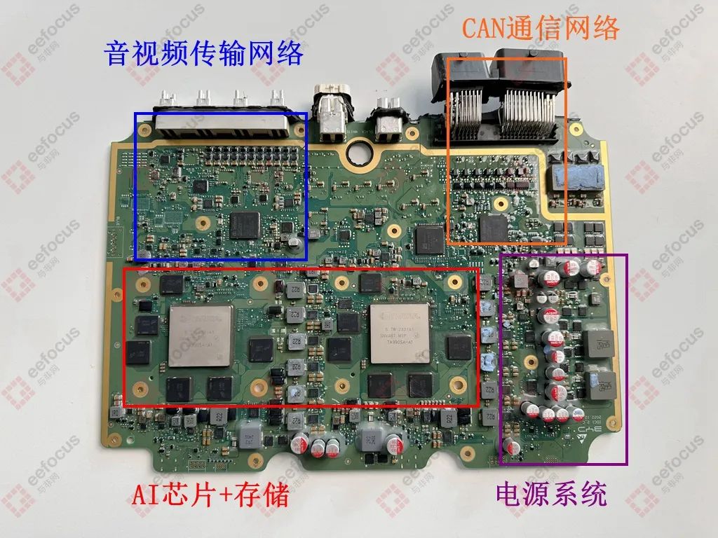
Through disassembly, we found that the ADAS board is impressive in both chip quantity and circuit layout, integrating key functional modules such as computational decision-making, real-time control, communication fusion control, and power systems. Compared to traditional fuel vehicles, the level of intelligence is vastly different. Let’s take a closer look at the hardware solutions for each functional part of the BYD Yangwang series ADAS board.
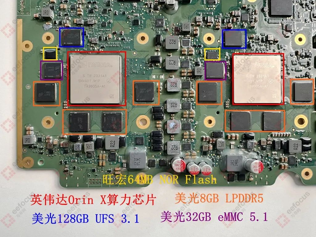
Computational Decision-Making
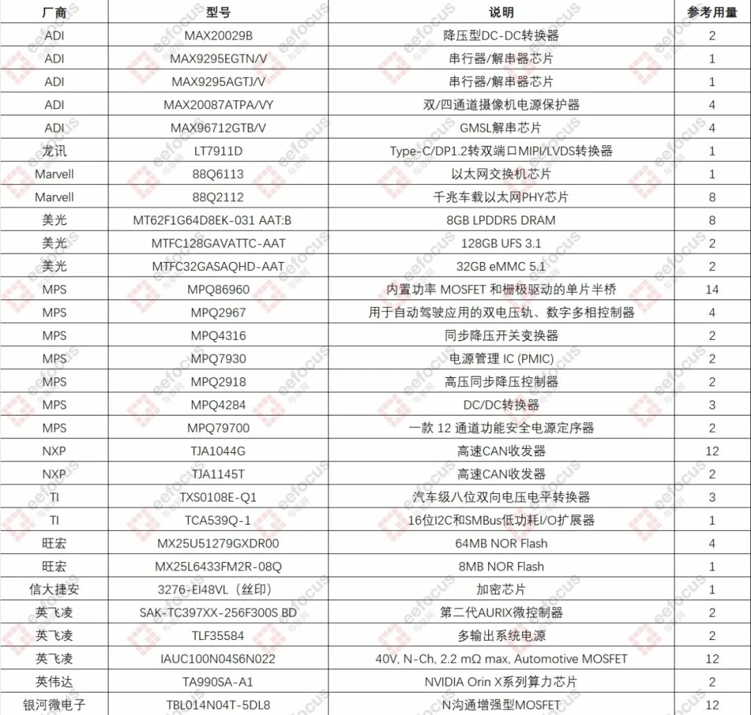
Two NVIDIA Orin X chips (TA990SA-A1) with a 7nm process, each capable of providing 254 TOPS of computational output;
Eight Micron LPDDR5 memory chips (MT62F1G64D8EK-031), totaling 64GB of memory, combined with high-speed transmission rates, ensuring real-time processing of multiple sensor data.
Storage System
Two Micron 128GB UFS 3.1 flash memory chips (MTFC128GAVATTC-AAT), used not only for local storage resources but also for high frame rate visual data caching;
Two Micron 32GB eMMC 5.1 chips (MTFC32GASAQHD-AAT), presumably used for storing core algorithm firmware;
Four Macronix NOR Flash chips (MX25U51279GXDR00), including two on the back of the board, primarily used to ensure the secure loading of boot code.
This tiered storage design, through differentiated configurations of storage media, achieves a good balance between performance and cost.
The previous circuit can be considered an integrated storage-computing circuit. Now let’s look at its power management system, which is also quite complex. From the BOM, it appears that multiple MPS chips collaboratively construct a complete power supply system.
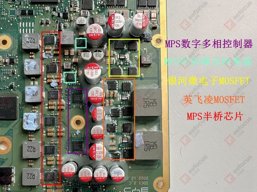
Power System
Four MPS digital multiphase controllers (MPQ2967), primarily used for dual voltage rails and digital multiphase control in autonomous driving applications.
Fourteen MPS half-bridge chips (MPQ86960), implementing a multiphase parallel power supply architecture, effectively controlling dynamic load adjustment rates.
Two MPS 12-channel functional safety power sequencers (MPQ79700), ensuring that the power-up sequence of each power rail strictly complies with standards. They also provide configurability and flexibility, supporting different applications and cross-generation design reuse of SoCs, integrating built-in self-test safety mechanisms to achieve high diagnostic coverage, ensuring the system meets the target automotive safety integrity level.
Twelve Infineon MOSFETs (IAUC100N04S6N022) and twelve Galaxy Microelectronics MOSFETs (TBL014N04T-5DL8) form a complementary pair, with the former’s 2.2mΩ ultra-low on-resistance significantly reducing switching losses, while the latter’s optimized gate charge characteristics enhance high-frequency response speed.
Two MPS synchronous buck converters (MPQ4316), internally integrating frequency-configurable synchronous buck switching converters with both high-side and low-side power MOSFETs. Using current control mode, they can provide up to 6A of efficient output current, with a wide input voltage range of 3.3V to 45V, making them suitable for various buck applications in automotive input environments.
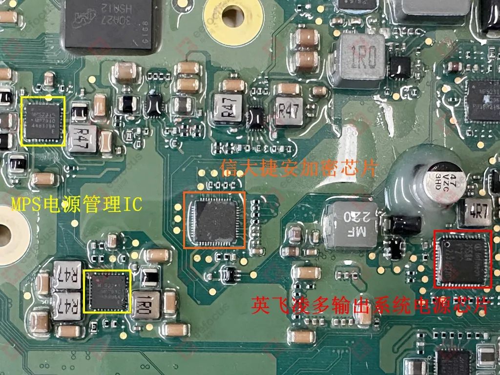
Two MPS power management chips (MPQ7930), suitable for various safety-related automotive systems, meeting the power management requirements of system processors.
Two Infineon multi-output system power chips (TLF35584), suitable for safety-related applications, providing 5V output voltage through an efficient and flexible front/back voltage regulator concept within a wide input voltage range, suitable for microcontrollers, various transceivers, and sensors.
Two MPS high-voltage synchronous buck controllers (MPQ2918), with a wide input voltage range of 4V-40V, using a PWM current control architecture, featuring precise cycle-by-cycle current limit protection, capable of driving dual N-channel MOSFETs.
One Xindajiean encryption chip (3276-EI48VL), ensuring data communication security through national cryptographic algorithms.
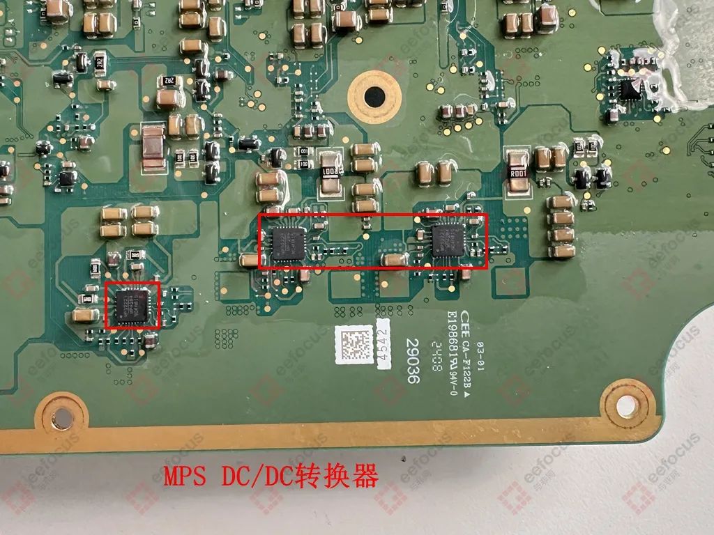
Three MPS DC/DC converters (MPQ4284).
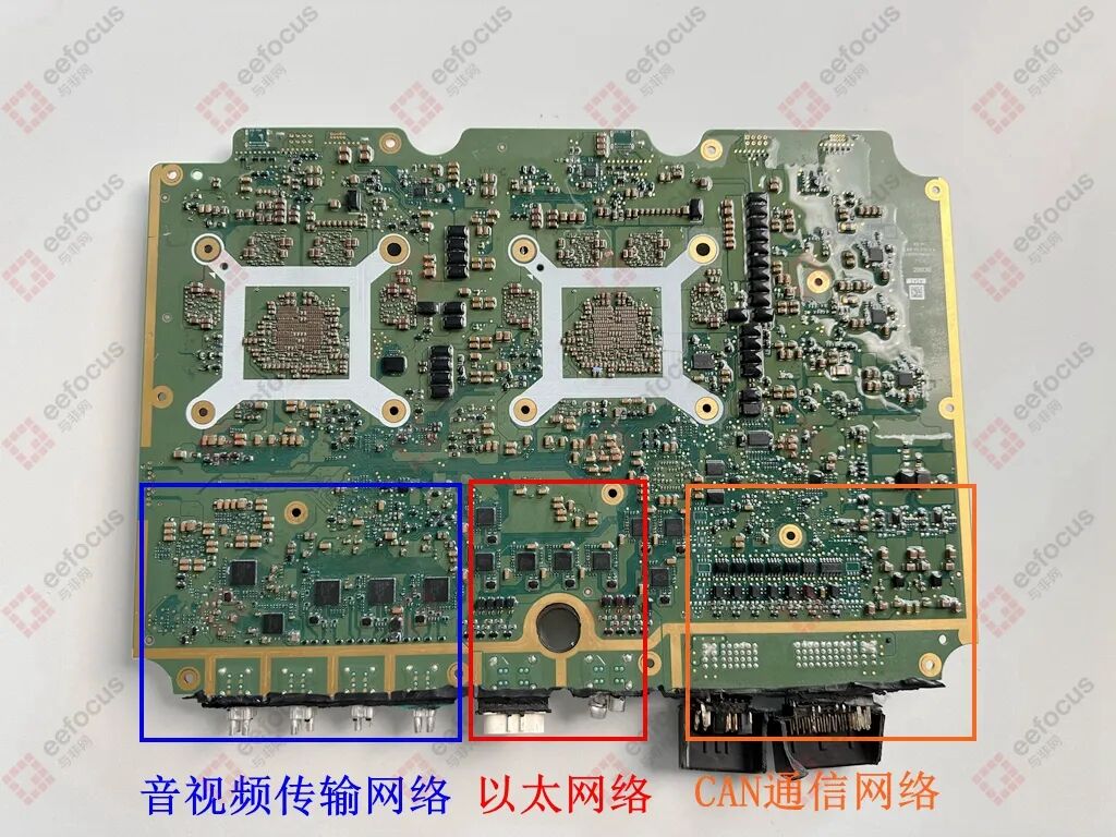
In-vehicle Communication Network
The in-vehicle communication network is another important part of the intelligent driving domain controller. From the PCB board’s several large interfaces, it can be inferred that there will be at least Ethernet, CAN communication, and audio/video output interfaces. Let’s take a closer look at the chips in the corresponding areas of the board.
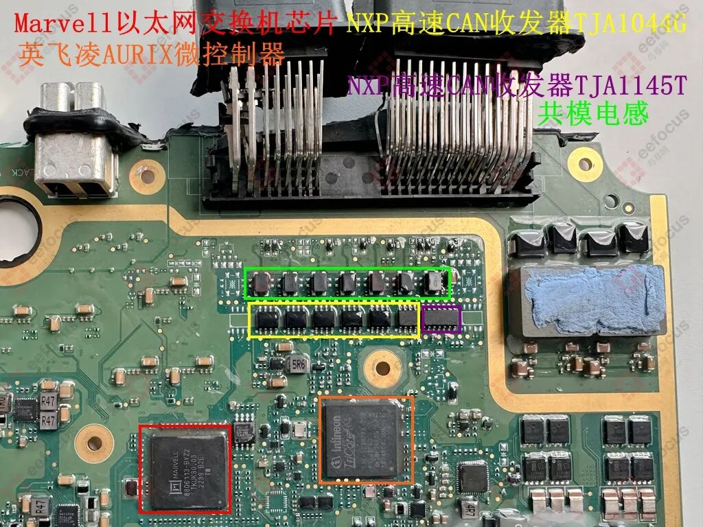
One Marvell Ethernet switch chip (88Q6113), essentially the backbone network of the vehicle’s TSN, supporting time-sensitive traffic scheduling and media access control security protocols (MACsec) hardware encryption.
Two second-generation Infineon AURIX microcontrollers (SAK-TC397XX-256F300S BD), with improvements in performance, storage capacity, connectivity, and scalability, and equipped with security protection mechanisms, achieving ASIL-D level functional safety based on a Lockstep core architecture to address new trends in the automotive industry.
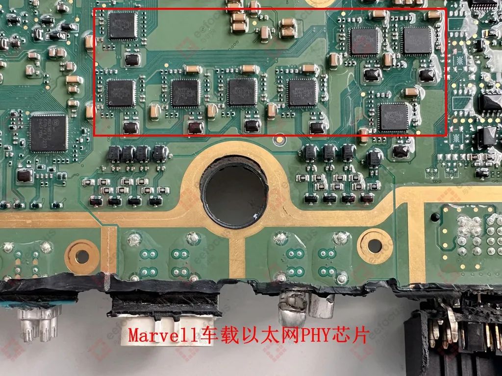
Eight Marvell automotive Ethernet PHY chips (88Q2112), working together with the above Marvell Ethernet switch chip to construct a high-data transmission channel.
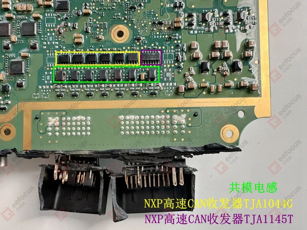
In terms of traditional CAN bus, two SOP14 packaged NXP high-speed CAN transceivers (TJA1145T) and twelve SOP8 packaged NXP high-speed CAN transceivers (TJA1044G), along with fourteen common-mode inductors, form a dual network architecture that maintains high-speed communication capability while controlling static power consumption to a very low level through low-power technology (PN mechanism).
In the design of audio/video input/output interfaces, the main components are ADI’s serializer/deserializer chips. What specific chips are involved?
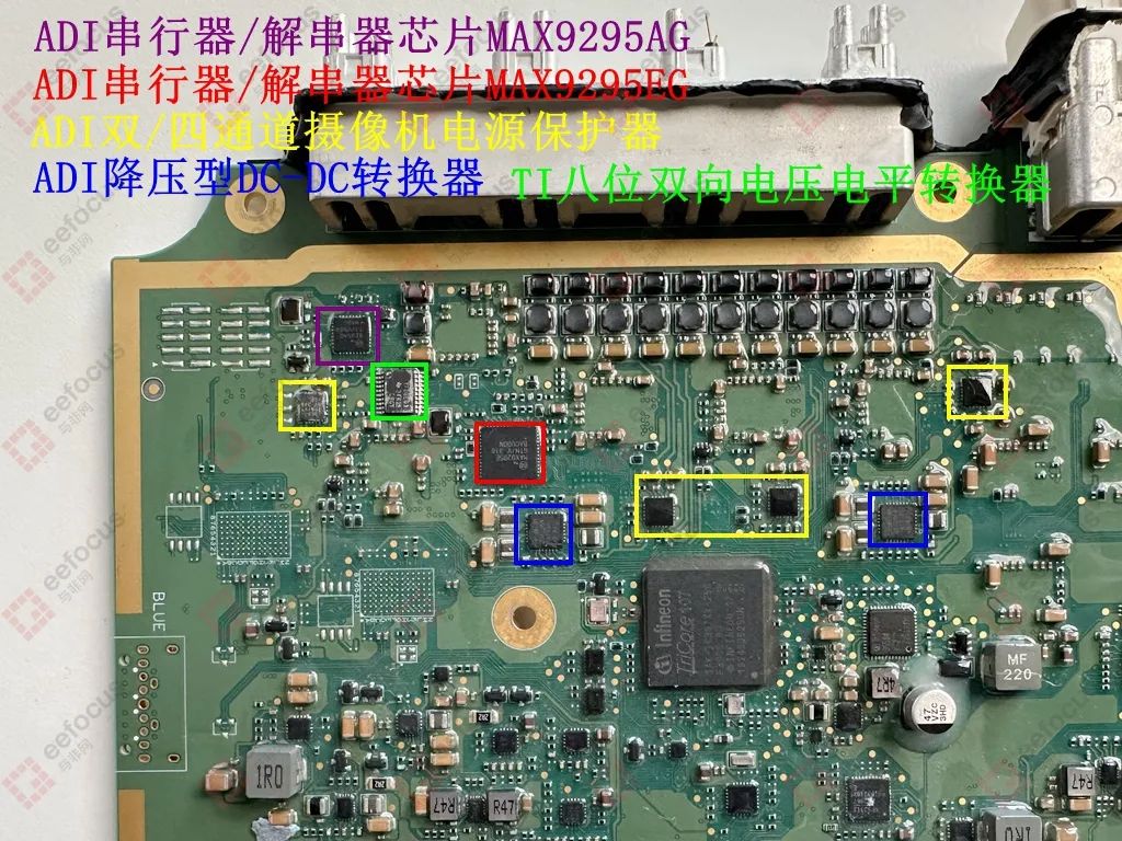
Two ADI MAX9295 series serializer/deserializer chips, with the larger package specifically being MAX9295EG and the smaller package being MAX9295AG.
Four ADI dual/four-channel camera power protectors (MAX20087), ensuring stable operation of high-definition cameras.
Two ADI buck DC-DC converters (MAX20029B), primarily for automotive applications, integrating four power rails and high operating frequency to minimize solution size, suitable for multi-rail load point regulation.
Three TI level shifters (TXS0108E), with 8-bit bidirectional voltage conversion capability effectively solving signal compatibility issues between devices in different voltage domains.
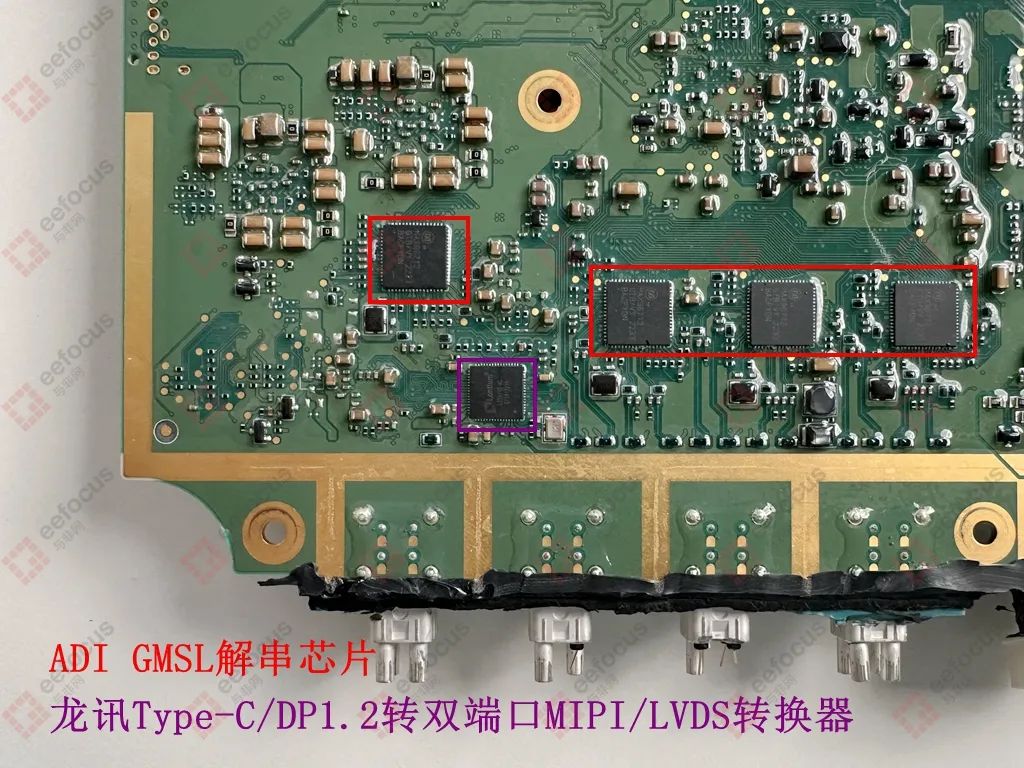
Four ADI GMSL deserializer chips (MAX96712).
GMSL is a high-speed serial interface suitable for the transmission of video, audio, and control signals. Combined with the previous two ADI serializer/deserializer chips, it can achieve high data transmission rates, meeting the needs for high-definition video and image transmission.
One domestic chip Longxun LT7911D, a Type-C/DP1.2 to dual-port MIPI/LVDS converter chip, for example, the display subsystem can use it to convert Type-C to dual MIPI, with high-definition output capabilities meeting the display requirements of AR-HUD.
In summary, the main chip BOM of the BYD Yangwang intelligent driving control domain is as follows, for reference only:
Conclusion
Through the disassembly of the BYD Yangwang ADAS board, we can categorize the main hardware into the following parts: First, the computational architecture and control aspects, where BYD, while pursuing peak computational power, does not forget the fundamental need for functional safety. The combination design of NVIDIA’s Orin X and Infineon’s AURIX microcontroller meets the parallel computing needs of deep learning algorithms while ensuring real-time response of control commands. In terms of energy efficiency management, the MPS multiphase power supply solution and the combination of Infineon and Galaxy Microelectronics power devices elevate the overall board power efficiency to the industry’s top tier. Regarding communication reliability, the hybrid network of TSN and CAN FD effectively reduces the transmission delay of critical control commands. Notably, the domestic substitution process is also accelerating, with the application of Galaxy Microelectronics MOSFETs and Longxun video interface chips indicating that the local supply chain has the capability to participate in core system design. We are fortunate to see leading domestic automakers steadily advancing the localization of chips while adopting top international chips. In the increasingly competitive landscape of smart vehicles, this deep vertical integration capability is key to the Chinese automotive industry’s ability to overtake in the curve. What are your thoughts on the hardware solutions of this ADAS board? Feel free to leave a comment for discussion!
Click to play
Prize Quiz
What are your thoughts on the hardware solutions of this ADAS board? Feel free to leave a comment for discussion!
Eefocus will randomly select one lucky user to win a BKT ergonomic lumbar support chair.
The answer to the next disassembly will reveal the winner.
Last issue’s winner list:

END
Note: The cover image of this article is from freepik, self-made by the author, and publicly authorized media materials.
Welcome to leave comments for exchange!


Industry Community


Related Articles
Espressif ESP32-S3-BOX-3 Disassembly Review – Domestic Chips Achieve AIOT Dominance
Antique Car Charger Head Disassembly: Ubiquitous Domestic Chips
19.99 Yuan “Apple” TWS Noise-Canceling Earbuds Disassembly: Domestic Chips Unbeatable
Author’s Column
Tap “Looking“↘ to share your world with friends
 Please click “Read the original” to see more news