Abstract:
In response to the current issues of low sampling rates and poor portability in signal acquisition systems, a design for a high-speed portable signal acquisition system based on FPGA is proposed. This design uses an FPGA chip to control an analog-to-digital converter (ADC) chip for high-speed signal sampling, then stores the data in a NAND Flash chip using DMA mode, and allows for real-time viewing of the collected signals through an LCD screen. First, the overall design framework of the system is described, followed by an introduction to the hardware design and implementation of each module, and finally, the test results of the signal acquisition system based on ultrasonic signals are presented. Experimental results show that this system can stably perform long-term, multi-batch data acquisition at a high sampling rate.
Citation Format in Chinese: Zhou Hao, Wang Haoquan, Ren Shilei. Design of portable signal acquisition system based on FPGA and NAND Flash[J]. Application of Electronic Technique, 2018, 44(9): 82-86.Citation Format in English: Zhou Hao, Wang Haoquan, Ren Shilei. Design of portable signal acquisition system based on FPGA and NAND Flash[J]. Application of Electronic Technique, 2018, 44(9): 82-86.
1 Introduction
With the rapid development of modern detection technology and scientific levels, the application scope of signal acquisition technology is becoming increasingly broad[1]. At the same time, higher requirements have been proposed for the design of signal acquisition systems regarding acquisition precision, sampling rates, and portability. Field Programmable Gate Arrays (FPGAs) have abundant logic gates, high clock frequencies, fast speeds, high efficiency, and rich IP cores, making them an effective means for designing high-speed signal acquisition systems[2-3]. This paper mainly introduces how to improve the sampling rate and portability of signal acquisition systems in response to current design needs.
Currently, the low sampling rate of portable signal acquisition systems is mainly limited by insufficient transmission speed and processing speed. A review of relevant literature in recent years shows that there are mainly two design schemes for FPGA-based signal acquisition systems: Scheme One uses FPGA as the logic control module, paired with an ADC acquisition module and a USB2.0 transmission module[4]; Scheme Two also uses FPGA as the logic control module, paired with DDR2/DDR3 modules to cache data collected by the ADC module at high speed[5-6]. Scheme One is limited by the transmission speed of USB, resulting in a lower sampling rate[7-8]; Scheme Two can achieve a higher sampling rate, but has issues of data volatility and small storage capacity, leading to insufficient portability[9].
To address these issues, this paper proposes a design scheme for a portable high-speed signal acquisition system, leveraging the high-speed storage characteristics of NAND Flash. The key to this design is to utilize the fast write speed of the storage chip and the reusability of the data bus, allowing the signals captured by the ADC to be stored in the storage chip via DMA mode. Additionally, this design configures an LCD display for real-time signal viewing, reducing the need for a host computer. The system meets the requirements for long-term, multi-batch signal acquisition.
1.1 Overall System Design Scheme
According to functionality and principles, the system is divided into four modules: a logic control module based on FPGA chips, a data conversion module centered on ADC chips, a high-speed data storage module centered on NAND Flash chips, and an LCD touch display module, as shown in Figure 1.
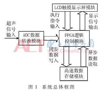
The basic working principle of the system: First, the analog-to-digital conversion module converts the received analog signal into a digital signal and sends it to the FIFO in the FPGA logic control module; then, the FPGA logic control module uses Direct Memory Access (DMA) mode to transfer data from the FIFO to the NAND Flash data storage module; next, the NAND Flash module performs high-speed data storage synchronously based on its internal structure; finally, the LCD module sends corresponding instructions to read data at a certain speed, processes the signals through the FPGA, and displays them on the LCD screen.
2 Hardware Circuit Design
2.1 FPGA Logic Control Module
The FPGA logic control module consists of ALTERA’s EP4CE40F29C8N, EPCS64SI16, and Hynix’s H27U1G8F2B chips. Among them, EP4CE40F29C8N is a Cyclone IV series FPGA chip with a maximum clock frequency of 472 MHz and 533 IO interfaces, meeting the system’s required maximum clock frequency and peripheral connection interfaces. The logic control module includes the top-level design part, system clock and reset part, acquisition control part, storage control part, LCD display control part, and NIOS II part, where the top-level design part is responsible for connecting various parts and interfacing the logic control module with other modules. The FPGA top-level schematic is shown in Figure 2.
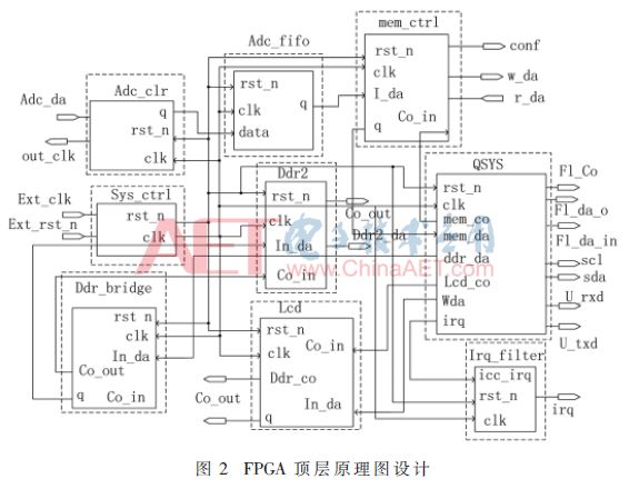
In the system clock and reset part, the FPGA chip’s system clock interface obtains a 25 MHz clock signal through a 25 MHz passive crystal oscillator, and the “PLL” IP core multiplies the 25 MHz clock signal to 33 MHz, 50 MHz, 100 MHz, and 200 MHz, which serve as the system’s clock circuit. Additionally, an asynchronous reset signal is generated for synchronous release.
The LCD display control part consists of a waveform module, data caching module, LCD display driver module, and touch screen instruction receiving module. This part provides an interface to output display data from QSYS to the DDR2 caching module; and establishes a DMA communication mechanism between the DDR2 chip and the LCD display chip to achieve display data output.
Using the QSYS system integration development tool, a NIOS II on-chip embedded processing system is established, responsible for receiving instructions and controlling program execution for the signal acquisition system. The NIOS II system performs the following tasks: (1) executes the system initialization program, listening for LCD instruction input; (2) implements read and write operations for configuring the Flash chip (H27U1G8F2B), configuring background images, font libraries, and the starting and ending positions of data storage in the collected batch number during the acquisition process; (3) implements data reading operations and converts collected signal data into waveform display data; (4) outputs control instructions for various peripheral drivers of the system.
2.2 Analog-to-Digital Conversion Module
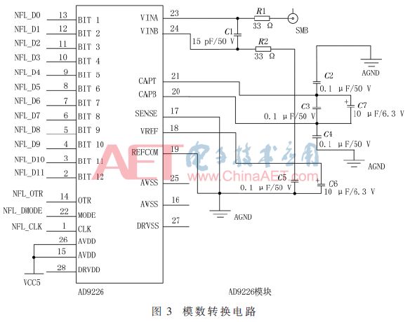
The analog-to-digital conversion circuit uses AD9226 as the conversion chip, which is a low-power (475 mW), high-precision (12 bit) high-speed ADC chip with a maximum conversion rate of 65 MSPS and a good signal-to-noise ratio (70 dB). In this design, the signal input range is 1 V~3 V. The sampling clock for this module is provided by the FPGA logic module to control the sampling rate; in all tests in this paper, the sampling rate is 50 MHz, and the circuit diagram for the analog-to-digital conversion module is shown in Figure 3.
2.3 High-Speed Data Storage Module
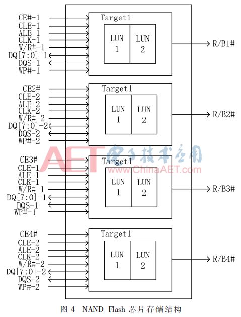
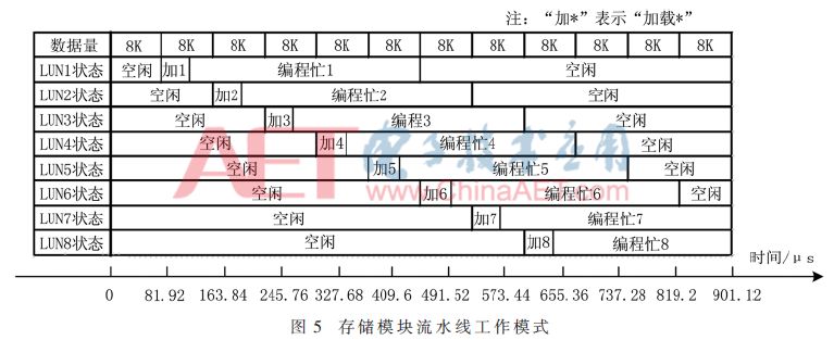
To match the high sampling rate, the high-speed data storage module selects SLC NAND Flash chips[10]. This design chooses Micron’s MT29F256G08AUCABH3 chip, which can achieve a pin read and write speed of 200 MT/s in synchronous mode, and uses DDR mode during data writing, meaning data is written on both the rising and falling edges of the clock. Analyzing its datasheet, since NAND Flash requires PROGRAM PAGE operations, writing 1 page of data (8 KB) with this chip takes about 400 μs. During this period, the ADC signal acquisition module collects 4×10⁴ B of data, which far exceeds the storage capacity of NAND Flash, failing to meet the design requirements of the system. Considering that the NAND Flash chip requires 40.96 μs to load 8 KB of data during synchronous writes, and the analog-to-digital conversion module requires 81.92 μs to collect 8 KB of data, the main factor affecting the system’s storage time is the programming time of the NAND Flash (350 μs).
To address this issue, this design combines the storage structure characteristics of MT29F256G08AUCABH3, as shown in Figure 4. This chip has an internal structure of 8 LUNs, and while one LUN is in programming state, other LUNs can perform read and write operations. Based on this feature, this design arranges the 8 internal LUN chips in a pipeline manner to sequentially perform data storage operations, as shown in Figure 5. When the collected data reaches 8 KB, the LUN in write preparation state begins to write data in DDR mode. After completing the writing of 1 page of data (8 KB), the next LUN enters the write preparation state, waiting for the next batch of data to reach 8 KB again. This process is repeated, and when the 8th LUN completes the write operation, the 1st LUN completes the programming process and can perform write operations while idle. Figure 5 illustrates the pipeline working mode of the storage chip.
2.4 Display Module
In the system’s display module, a 7-inch LCD screen with a resolution of 800×480 and digital interface drive is selected. The output color signal of the display screen is transmitted through 565 RGB parallel digital signals, paired with a 512 MB DDR2 SDRAM chip for caching display data. The clock frequency of the system display module is 33 MHz.
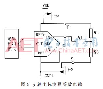
In addition to the display function, this module also serves the human-computer interaction function. Utilizing the characteristics of the touch screen, it completes the control of the entire system’s operation, reducing the need for a keyboard module and simplifying operation. This design uses a resistive touch screen, where each of the x and y axes has two signal lines connected to a dedicated ADC chip (this design uses the AW2083 chip). Each time the touch screen is pressed, a resistance value is generated between the corresponding x and y axes. By applying a reference voltage between the positive and negative terminals of the two coordinate axes, when a position on one coordinate axis is touched, the resistance between that position and the corresponding positive and negative terminals will feedback to the ADC’s input in the form of voltage, generating a 12-bit AD quantization value. The coordinate data collected by the AD chip is proportional to the actual coordinate value and has a linear relationship. Figure 6 shows the equivalent circuit diagram of y-axis coordinate measurement.
3 System Program Logic Design
When the system is powered on, it performs initialization operations. The FPGA reads the configuration information from the NAND Flash chip. It retrieves the initialization interface of the display module for output and display, while obtaining the next storage address from the configuration chip. After the system initialization is completed, it enters standby mode, listening for instruction inputs from the LCD display module.
3.1 Signal Acquisition Process
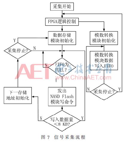
By clicking the “Start Acquisition” button on the LCD module, the signal acquisition program is triggered. The logic control module detects the signal acquisition start instruction, and the system enters the signal acquisition process.
Signal acquisition process:
(1) The high-speed storage module initializes, activating the storage state of the next LUN following the previous batch’s completion.
(2) The logic control module sends an enable signal to the mode conversion module while inputting a 50 MHz clock signal to the analog-to-digital conversion module.
(3) The analog-to-digital conversion module begins working, converting the input analog signal into a 12-bit digital signal at a conversion rate of 50 MS/s, and outputs it to the logic control module.
(4) After receiving the 12 bits, the logic control module left-shifts it by 4 bits and adds it to the 4-bit binary value of the current acquisition batch to generate a 16-bit value stored in the FIFO. The FIFO is set for 16-bit input signals at a frequency of 50 MHz; the output signal is 8 bits, with an output signal frequency of 400 MHz; depth is 4,096 words.
(5) When the FIFO status is “FULL,” the logic control module sends a write command to the high-speed data storage module and sends a read command to the FIFO, initiating the system’s DMA transfer of data from the FIFO to the high-speed data storage module.
(6) After completing the page data storage, the logic control module disables FIFO read enable. The high-speed data storage module activates the storage state of the next LUN, repeating steps (5) to (6). The signal acquisition flowchart is shown in Figure 7.
3.2 Signal Acquisition Stop Process
When the “Stop Acquisition” button on the LCD display module is triggered, the logic control module waits for the data acquisition process in step (6) to execute, disabling the high-speed data storage module and the analog-to-digital conversion module, while storing the current acquisition batch number and the corresponding starting and ending positions of the data in the configuration information storage Flash. The system enters standby mode, listening for instruction inputs from the LCD display module, while initializing the display module’s interface.
3.3 Waveform Display Process
After triggering the waveform display button on the LCD, the interface switches to the batch selection interface, allowing the user to click and select the corresponding batch for waveform display, entering the waveform display operation process.
Waveform display process:
(1) The logic control module reads the starting and ending positions of the corresponding batch data acquisition from the configuration Flash.
(2) It reads the data from the corresponding address in the high-speed storage module and writes it into the waveform control IP core. The waveform control module is responsible for controlling the LCD waveform window and latching the collected data values into dual-port RAM, while also outputting the display coordinates and waveform display clock frequency.
(3) The data from the waveform control module is input into the DDR2 chip in the LCD display module.
(4) The LCD screen reads the data from the DDR2 for display.
(5) When all data for the corresponding batch has been read, the waveform display process ends.
3.4 High-Speed Data Storage Control Process
The high-speed data storage control program is mainly divided into the data acquisition write process and the display data read process. In this design, the data acquisition write process uses synchronous writing at a working frequency of 200 MHz; the display data read process uses asynchronous reading at a working frequency of 50 MHz.
(1) High-speed data write process: (i) The NAND Flash chip activates synchronous read and write status; (ii) obtains the write page address from the logic control module; (iii) sends a write operation command to the NAND Flash; (iv) writes the write operation address to the NAND Flash; (v) NAND Flash waits for data write enable; (vi) upon receiving the write enable from the logic control module, it begins writing data; (vii) when a page of data is filled, that LUN enters programming state, while obtaining the storage address of the next LUN from the logic control module, repeating steps (iii) to (vii).
(2) High-speed data read process: (i) The NAND Flash chip activates asynchronous read and write status; (ii) obtains the read page address from the logic control module; (iii) sends a read operation command to the NAND Flash chip; (iv) writes multiple operation addresses to the NAND Flash; (v) reads NAND Flash data and sends it to the logic control module; (vi) when a page of data has been read, repeat steps (ii) to (vi).
4 Experimental Testing
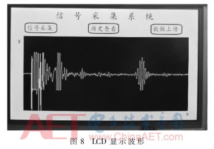
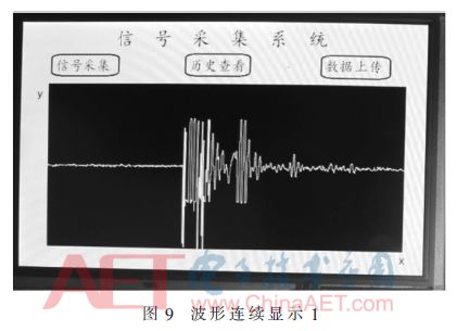
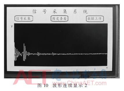
The testing platform consists of an ultrasonic transmitting circuit, an ultrasonic receiving circuit, an ultrasonic probe, and a metal sheet with weld seams. The ultrasonic probe emits a 2.5 MHz ultrasonic signal to the metal sheet. When the ultrasonic signal reaches the weld seam, part or all of the signal reflects, generating an echo signal. The signal acquisition system collects the echo signal through the ultrasonic receiving circuit, processes it through the logic control module, and writes it into the storage module. Simultaneously, the processed data is displayed on the LCD screen. Figure 8 shows the output waveform of the signal detection system. Comparing the two waveforms reveals that the system can perform good sampling at a sampling rate of 50 MHz. Figures 9 and 10 show the continuous sampling data waveform output, achieving continuous multi-batch signal acquisition.
5 Conclusion
This system utilizes the AD9226 high-speed analog-to-digital conversion module to convert the collected analog signals into digital signals, which are then stored in high-capacity NAND Flash via FPGA and displayed as waveforms on an LCD screen. In practical applications, this system can perform continuous long-term multi-batch high-speed signal acquisition, with characteristics of compactness and portability.
References
[1] Zhang Xiaowei, Su Shujing. Design of high-speed and high-precision data acquisition system based on FPGA[J]. Instrument Technology and Sensor, 2016(1): 70-72.
[2] BAO S, YAN H, CHI Q, et al. FPGA-based reconfigurable data acquisition system for industrial sensors[J]. IEEE Transactions on Industrial Informatics, 2017, 13(4): 1503-1512.
[3] Yang Haigang, Sun Jiabin, Wang Wei. Overview of FPGA device design technology development[J]. Journal of Electronics and Information Technology, 2010, 32(3): 714-727.
[4] XU Z, ZHU L, SHAN J F, et al. A new high-speed data acquisition system[J]. Journal of Fusion Energy, 2015, 34(3): 1-4.
[5] Huang Yuanwang, Yan Jihong, Zhou Wei. Design of data acquisition testing system based on FPGA[J]. Modern Radar, 2015, 37(4): 73-76.
[6] KHEDKAR A A, KHADE R H. High-speed FPGA-based data acquisition system[J]. Microprocessors & Microsystems, 2016, 49: 87-94.
[7] Li Mao, Yang Lu, Zhang Yanhua. Design of multi-channel ultrasonic detection system based on FPGA and USB[J]. Instrument Technology and Sensor, 2017(8): 82-84.
[8] Meng Xiaodong. Design and verification of FPGA-based DDR3 controller[D]. Changsha: National University of Defense Technology, 2012.
[9] LIU D, WANG Y, QIN Z, et al. A space reuse strategy for Flash translation layers in SLC NAND Flash memory storage systems[J]. IEEE Transactions on Very Large Scale Integration Systems, 2012, 20(6): 1094-1107.
[10] Xiao Jia. Design and implementation of high-speed storage system based on NAND Flash for big data[D]. Xi’an: Xi’an University of Electronic Science and Technology, 2014.
Author Information:
Zhou Hao, Wang Haoquan, Ren Shilei
(College of Information and Communication Engineering, North University of China, Taiyuan, Shanxi 030051)