
To continuously improve various features in next-generation devices, wearable and hearable devices rely on memory. Memory is a key design factor for implementing advanced devices…
Although wearable and hearable technologies may seem like extensions of the previous generation of handheld devices, the innovative features required to enhance their value, user experience, and functionality significantly increase complexity. For example, adding stylish features and functions to smartwatches within stringent size and power constraints.
Therefore, when considering smaller devices (such as hearing aids and earbuds), we must meet stricter limitations, especially regarding product weight. To facilitate easy implementation of revisions and continuous improvements of these product features in next-generation devices, wearable and hearable devices depend on memory. Memory is a key design factor for achieving these advanced devices.
Features Required for Providing an Excellent User Experience
Adding innovative features to systems can significantly increase program code size. For instance, vital sign monitoring requires more data storage to implement additional designs, such as security, wireless OTA updates, data logging, and artificial intelligence (AI).
Next, security becomes increasingly important for every connected device and requires continuous updates. For wireless devices like smartwatches, these updates are often implemented using OTA mechanisms, which require sufficient memory to maintain and verify secure program code images before transferring control to the new program code.
Many devices are also beginning to implement data logging. The impact of recording user experiences is just beginning to be explored, leading to a new range of customizable features. Current tracking devices (such as health monitors) will adopt more sensors to capture more data.
For the next generation of these devices, Edge AI will become a disruptive trend, leading to increased demands for memory size. These edge devices use advanced AI systems to execute machine learning (ML) algorithms to locally process data on the device, enabling functionalities like voice recognition, facial recognition, fingerprint detection, and health monitoring. Due to their low cost, small size, and high energy efficiency, these devices rely on microcontrollers (MCUs) to execute complex ML algorithms. MCUs deploy dedicated cores for parallel processing, allowing ML models to run and optimize on the device itself.
The Role of Memory in Product Differentiation
All these new features drive the demand for more non-volatile memory, meaning that memory retains stored data even during power outages. Since many wearable and hearable devices are battery-powered, NOR Flash is often the preferred memory due to its fast read access, durability, and reliability.
In fact, the NOR Flash market for smartwatches, wireless earbuds, and other wearable devices is expected to grow from $90 million in 2019 to over $265 million by 2024 (data source: Gartner, ABI, and Infineon internal estimates). This growth is driven by increasing memory demands from connected devices in automotive, medical, and industrial sectors. Simultaneously, density demands are expected to rise, with wearables transitioning from lower density 64Mb memory to medium density 256Mb.
The physical size can be said to be the most critical aspect of this memory, as chip size directly determines cost, the space occupied by the final component, and the form factor of the end product. One of the unique requirements for hearable and wearable devices is that the height or profile of the storage device is crucial. Therefore, the depth of memory chips must also be optimized, with weight being critical in certain applications, such as hearable devices.
For these reasons, memory manufacturers are continuously developing innovative technologies and new architectures to improve die size and power consumption. For example, the SEMPER NOR Flash series utilizes proprietary MIRRORBIT technology to store two bits of data in each cell, effectively doubling the density of the component memory section. The difference is significant as it allows for higher density memory in a smaller space. A typical 256Mb NOR Flash die size is about 18mm2. With MIRRORBIT technology, 256Mb can fit within a 13.6mm2 die.
Memory also needs to be provided to manufacturers as bare dies. Notably, the standard approach for wearable devices is to use custom packaging, such as wafer-level chip-scale packaging (WLCSP) with ball grid array (BGA) connections. In short, manufacturers integrate multiple processors (e.g., CPU and DSP) with their chosen memory die in a single package, known as system-in-package (SiP), as shown in Figure 1. This, in turn, leads to the need for higher density memory components, as they now need to store application code and data for two processors. To achieve these SiP components, SEMPER Nano is offered in a known good die (KGD) format, allowing OEM manufacturers to integrate it with their chosen processors.
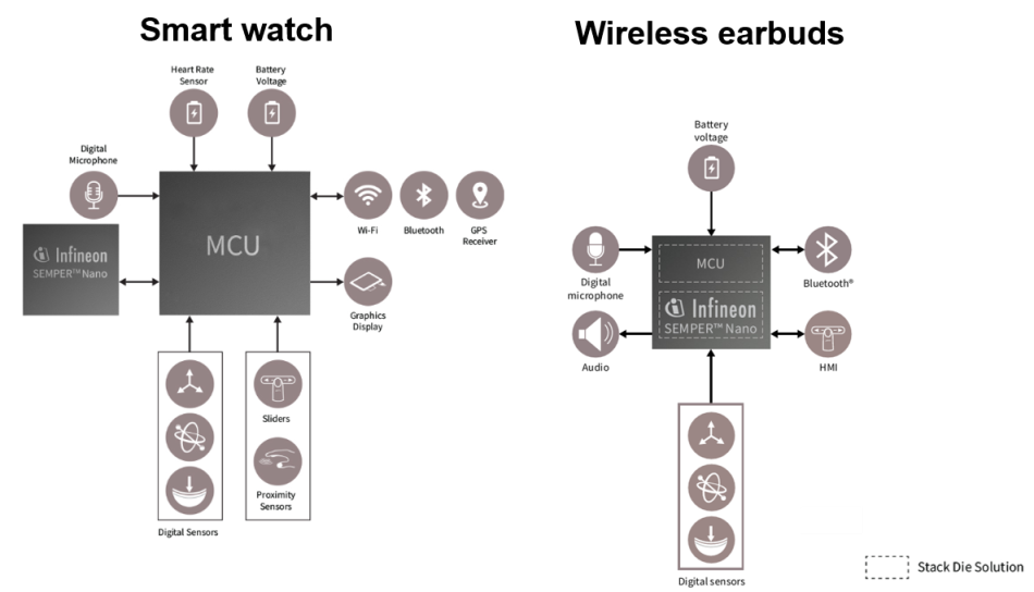 Figure 1:Traditional hearable and wearable devices require external NOR Flash to store program code, data, and data logs (left). Space-constrained applications, such as wireless earbuds with true wireless stereo (TWS) functionality, utilize high-density stacked chip architectures to integrate MCUs and DSPs with memory in a chip-scale package (right). (Image source: Infineon Technologies)
Optimizations for Lower Power Consumption
Traditionally, memory has been designed as a commodity for a wide range of applications. However, the stringent constraints of the hearable and wearable device market demand memory that is explicitly optimized for size, power, and reliability.
There are multiple ways to optimize NOR Flash to minimize power consumption. Traditionally, low power is achieved by reducing standby current and active read current. Deep sleep modes can significantly extend battery life, further enhancing power efficiency. In other words, the typical standby current of SEMPER Nano NOR Flash is 5.0µA, which is 54% lower than that of SEMPER NOR Flash, with typical deep sleep mode dropping to 1µA, 23% lower than SEMPER NOR Flash (Figure 2).
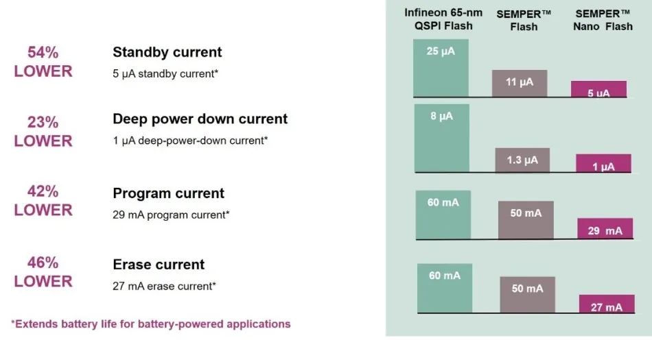 Figure 2:Comparison of power consumption between SEMPER Nano NOR Flash and SEMPER NOR Flash. (Image source: Infineon Technologies)
The key to reducing power consumption is to minimize the time it takes for memory to transition from active mode to standby mode. To maximize energy savings, memory needs to be able to enter standby mode immediately to avoid unnecessary power waste (Figure 3).
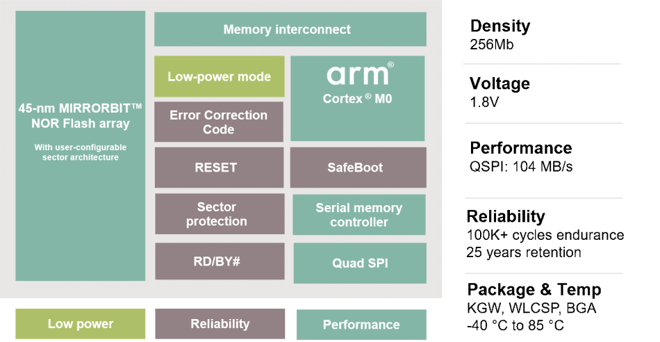 Figure 3:SEMPER Nano NOR Flash integrates a processor that alleviates the power and reliability processing burden on the application CPU. (Image source: Infineon Technologies)
Fast read access is crucial for features like ‘instant-on’. No one wants to wait for their earbuds to start up. Here, NOR Flash is built on an internal parallel array interface to achieve fast read times, enabling faster startup of larger programs.
The fast access and low power of NOR Flash make it possible to execute program code directly from Flash, known as execute-in-place (XiP), which further reduces the time it takes for devices to power on. This unified memory approach combines program code, data, and logs into a single memory chip. It significantly reduces the overall physical memory footprint by eliminating the RAM used for program code and data storage. It also enhances overall reliability, reduces power consumption, and achieves a smaller form factor with simplified designs.
Better Memory Equals Better Wearables
The key to achieving success and profitability in the wearable and hearable device market is to stand out with innovative features like advanced fitness and medical monitoring that provide an excellent user experience. These features increase the demand for higher density NOR Flash optimized for size, low power, and reliability. The reliability features integrated into NOR Flash—along with the ability to store program code, data, and logs in a single unified memory—simplify and accelerate designs while enabling developers to meet the stringent design constraints of these applications.
Linus Wong is the Product Management Director at Infineon Technologies
Wilson Yen is a Senior Application Manager at Infineon Technologies
This article was originally published in EDN America, reference link: How NOR flash helps overcome design challenges in wearables, translated by Susan Hong.