Welcome FPGA engineers to join the official WeChat technical group
Clickthe blue textto follow us at FPGA Home – the best and largest pure FPGA engineer community in China

Non-volatile storage components come in many forms, such as EPROM, EEPROM, NOR FLASH, and NAND FLASH. The first two have basically been phased out, so I will focus only on the latter two. This article provides a brief introduction to the basic storage unit structure, write operations, erase operations, and read operations of FLASH technology, as well as the characteristics and application scenarios determined by the storage structure of NOR and NAND, laying the groundwork for subsequent hardware design and driver programming.
1 Basic Storage Unit of FLASH – Floating Gate Field Effect Transistor
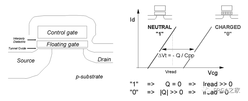
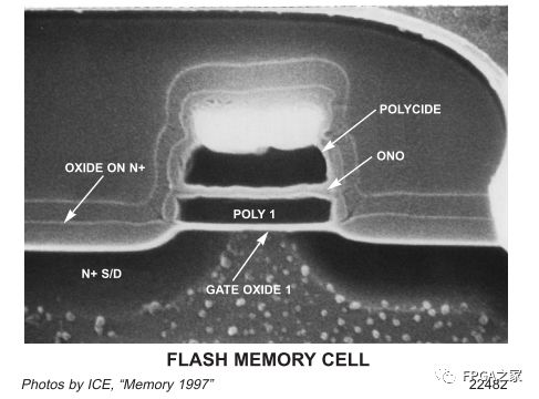
Both NOR FLASH and NAND FLASH use Floating Gate Field Effect Transistors (Floating Gate FET) as the basic storage unit to store data. The Floating Gate FET has four terminal electrodes: Source, Drain, Control Gate, and Floating Gate. The functions of the first three terminal electrodes are the same as those of a regular MOSFET, with the only difference being the floating gate. FLASH utilizes whether the floating gate stores charge to represent digital ‘0’ and ‘1’. When charge is injected into the floating gate, there is a conductive channel between D and S, reading ‘0’ from the D terminal; when there is no charge in the floating gate, there is no conductive channel between D and S, reading ‘1’ from the D terminal. The principle is illustrated in Figure 1.1[1], and Figure 1.2 is a cross-sectional view of an actual Floating Gate FET.
Note: SLC can be simply understood as using whether the floating gate stores charge to represent digital ‘0’ and ‘1’, while MLC uses the amount of charge in the floating gate to represent ’00’, ’01’, ’10’, and ’11’, with TLC being similar to MLC.
2 Operations of the Basic Storage Unit of FLASH – Write/Eras/Read
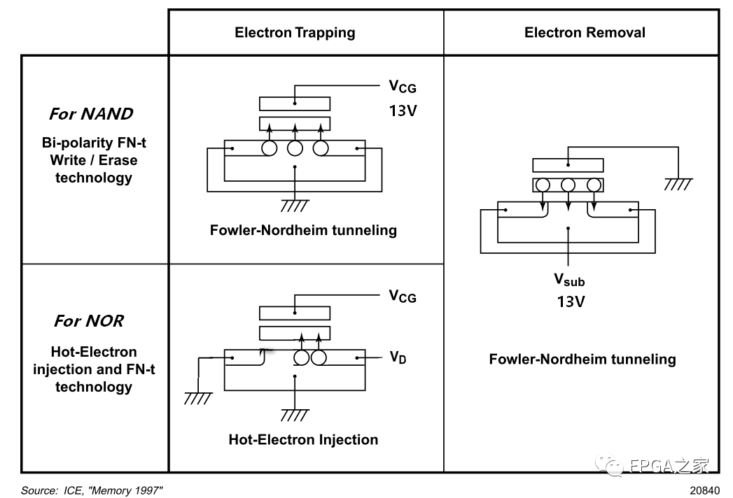
In FLASH, two common techniques for injecting charge into the floating gate are hot electron injection and Fowler Nordheim tunneling (F-N tunneling); the technique usually used to remove charge from the floating gate is also the F-N tunneling, with the basic principle illustrated in Figure 2[2].
The write operation is the process of injecting charge into the floating gate. NOR FLASH injects charge into the floating gate by hot electron injection (this method has a lower charge injection efficiency, hence NOR FLASH has a lower write speed), while NAND FLASH injects charge into the floating gate through F-N tunneling. Before writing, the original data must be erased (i.e., the charge in the floating gate must be removed), meaning that after erasing, all readouts from FLASH are ‘1’.
The erase operation is the process of removing charge from the floating gate, and both NOR FLASH and NAND FLASH remove charge from the floating gate through F-N tunneling.
During the read operation, the voltage applied to the control gate is very low, so it does not change the amount of charge in the floating gate, meaning that the read operation does not alter the existing data in FLASH. When there is charge in the floating gate, there is a conductive channel between D and S, reading ‘0’ from the D terminal; when there is no charge in the floating gate, there is no conductive channel between D and S, reading ‘1’ from the D terminal.
3 Structure and Characteristics of NOR FLASH and NAND FLASH
3.1 Structure and Characteristics of NOR FLASH
The structural principle diagram of NOR FLASH is shown in Figure 3.1, where each basic storage unit under a Bit Line is in parallel. When a certain Word Line is selected, reading of that Word can be achieved, which allows for bit reading (i.e., Random Access) and has a high read speed. Figure 3.1 is a schematic structure diagram of a 3*8bit NOR FLASH, and Figure 3.2 is a cross-sectional view along the Bit Line, illustrating the silicon cross-section of NOR FLASH. This parallel structure determines many characteristics of NOR FLASH.
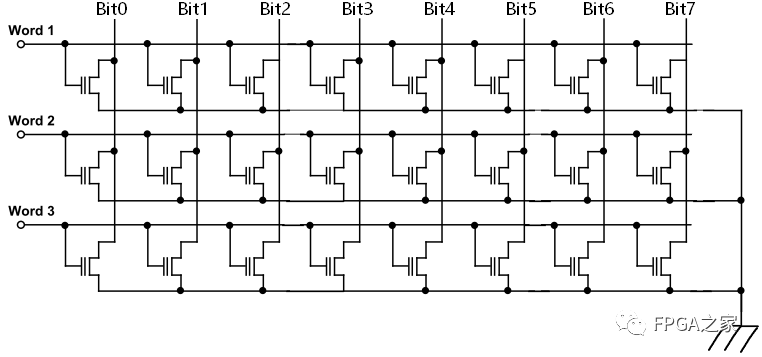
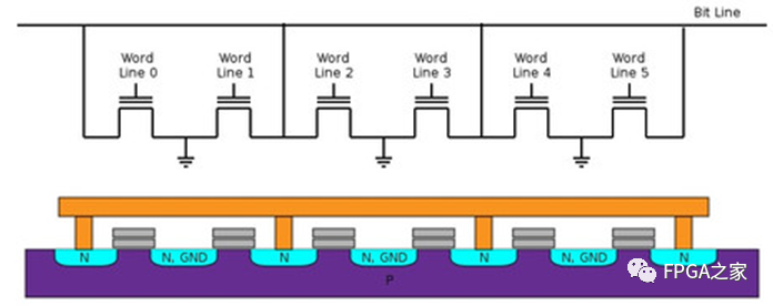
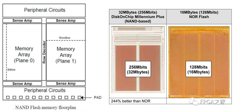
(1) The parallel structure of the basic storage unit results in a large area occupied by metal wires, leading to a lower storage density for NOR FLASH, making it unsuitable for applications requiring large-capacity storage. It is suitable for code-storage but not for data-storage, as seen in Figure 3.3[3].
(2) The parallel structure of the basic storage unit allows for independent addressing of storage units and high reading efficiency, making it suitable for code-storage, and programs can run directly in NOR (i.e., it has RAM characteristics).
(3) NOR FLASH uses hot electron injection for writing, which is less efficient, leading to a lower write speed, making it unsuitable for frequent erase/write scenarios.
Finally, a little tip: The ‘N’ in NOR FLASH means NOT, indicating that when there is charge in the Floating Gate, it reads ‘0’, and when there is no charge, it reads ‘1’, representing a ‘non’ logic; the ‘OR’ means that the basic storage units under the same Bit Line are in parallel, representing an ‘or’ logic, which is the origin of NOR.
3.2 Structure and Characteristics of NAND FLASH
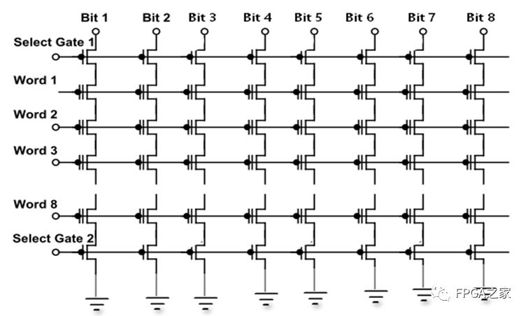
The structural principle diagram of NAND FLASH is shown in Figure 3.4, where each basic storage unit under a Bit Line is in series. The unit of data read by NAND is Page. When a certain Page needs to be read, the FLASH controller does not apply voltage to the Word Line of that Page but applies voltage to the Word Lines of all other Pages (the voltage value cannot change the amount of charge in the Floating Gate), allowing all basic storage units of these Pages to conduct D and S, while the conduction/off state of the basic storage unit of the Page we want to read depends on whether there is charge in the Floating Gate. If there is charge, the Bit Line reads ‘0’; if there is no charge, the Bit Line reads ‘1’, thus achieving the reading of Page data. It can be seen that NAND cannot achieve bit reading (i.e., Random Access), and program code cannot run on NAND.
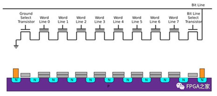
Figure 3.4 is a schematic structure diagram of an 8*8bit NAND FLASH, and Figure 3.5 is a cross-sectional view along the Bit Line, illustrating the silicon cross-section of NAND FLASH. The series structure of NAND FLASH determines many of its characteristics.
(1) The series structure of the basic storage unit reduces the area occupied by metal wires, resulting in a high utilization rate of the Die, hence NAND FLASH has a high storage density, suitable for applications requiring large-capacity storage, i.e., suitable for data-storage, as shown in Figure 3.3[3].
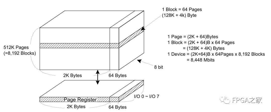
(2) The series structure of the basic storage unit means that NAND FLASH cannot perform bit reading and thus cannot achieve independent addressing of storage units, so programs cannot run directly in NAND. Therefore, NAND is read and written in Page units and erased in Block units, as shown in Figure 3.6.
(3) NAND FLASH uses F-N tunneling for writing, which is more efficient, thus NAND has a high erase/write speed, making it suitable for frequent erase/write scenarios. At the same time, NAND reads in Page units, so the read speed is also not low (slightly lower than NOR).
Finally, a little tip: The ‘N’ in NAND FLASH means NOT, indicating that when there is charge in the Floating Gate, it reads ‘0’, and when there is no charge, it reads ‘1’, representing a ‘non’ logic; the ‘AND’ means that the basic storage units under the same Bit Line are in series, representing an ‘and’ logic, which is the origin of NAND.
3.3 Comparison of NOR and NAND
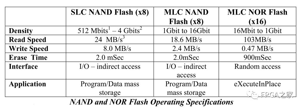
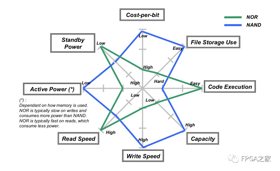
Through the analysis of the structures and characteristics of NOR and NAND in sections 3.1 and 3.2, we can draw conclusions from Figures 3.7[5] and 3.8[5]. For more detailed comparisons, please refer to reference [3].
4 Reliability Issues of FLASH Basic Storage Units

Welcome FPGA engineers and embedded engineers to follow our public account

The largest FPGA WeChat technical group in the country
Welcome everyone to join the national FPGA WeChat technical group, which has tens of thousands of engineers, a group of engineers who love technology. Here, FPGA engineers help each other and share knowledge, creating a strong technical atmosphere!Hurry up and invite your friends to join!!

Press and hold to join the national FPGA technical group
FPGA Home Component City
Advantageous component services, please scan the code to contact the group owner: Jin Juan Email: [email protected] Welcome recommendations to procurement
ACTEL, AD part advantages ordering (operating the full series):
XILINX, ALTERA advantageous stock or ordering (operating the full series):
(The above components are part of the models; for more models, please consult the group owner Jin Juan)
Service concept: FPGA Home Component City aims to provide engineers with fast and convenient component purchasing services. After years of dedicated service, our customer service covers large listed companies, military research units, and small and medium-sized enterprises across the country. Our biggest advantage is emphasizing a service-first approach and ensuring quick delivery and competitive prices!
Directly operated brands: Xilinx, ALTERA, ADI, TI, NXP, ST, E2V, Micron, and over a hundred other component brands, especially skilled in components subject to US embargo against China,we welcome engineer friends to recommend us to procurement or consult us directly!We will continue to provide the best service in the industry!

Official acknowledgment of FPGA technology group brands: Xilinx, Intel (Altera), Microsemi (Actel), Lattice, Vantis, Quicklogic, Lucent, etc.