1. What is a Download Circuit
The download circuit of a microcontroller refers to the hardware circuit used to download the written program (firmware) to the internal memory of the microcontroller. This process is often referred to as programming or flashing. The download circuit includes the debugging interface with the microcontroller and the corresponding circuit design, ensuring that data can be transmitted stably and reliably to the microcontroller’s flash memory or other types of storage.
2. Microcontroller’s Debugging Interface
The mainstream debugging interfaces mainly include two types: JTAG (Joint Test Action Group) and SWD (Serial Wire Debug). These interfaces can be connected to external debuggers/programmers (such as ST-Link, J-Link…) for program downloading and debugging.
Many beginners often get confused about various debuggers and debugging interfaces. We can divide this confusion into two parts: one part is the communication method between the computer and the microcontroller (debugging interface), and the other part is the hardware that acts as a communication bridge between the microcontroller and the computer (debugger).
The mainstream debugging interfaces are JTAG and SWD. The mainstream debuggers include the J-Link series, ST-LINK series… Most of these debuggers support both JTAG and SWD. As for why we only need a few wires to flash the program (SWD), but there are a lot of pins on the debugger, this is because debuggers are usually designed to be flexible enough to support various debugging and programming protocols, as well as to adapt to different target board requirements.
What are the Differences Between JTAG and SWD?
Which One Should We Choose?
JTAG Interface
JTAG (Joint Test Action Group) is a standardized testing interface originally designed for production testing of circuit boards, and later its use was expanded to programming, debugging, and simulation. The formal standard name of the JTAG interface is IEEE 1149.1, which defines the methods for testing circuit connectivity at the board and chip level.
Features of JTAG
Test Access Port (TAP): JTAG defines a test access port with several signal pins, the most important being TCK (Test Clock), TMS (Test Mode Select), TDI (Test Data Input), and TDO (Test Data Output). An optional fifth pin is nTRST, which is used for asynchronously resetting the TAP controller.
TAP Controller: The JTAG interface manages testing logic through a finite state machine (TAP controller). This state machine is controlled by TCK and TMS and completes different testing and programming operations through different state sequences.
Boundary Scan: JTAG uses boundary scan registers to access all I/O pins of the chip, allowing testing of connectivity between chip pins and between multiple chips. Through boundary scan, testing can be performed without interfering with the normal operation of the chip.
Chain Structure: Multiple JTAG-supported devices can be connected in series to form a debugging chain. In this way, multiple devices can be tested and debugged simultaneously using the same set of TAP signals.
Advantages:
1. Multi-device Chain: JTAG supports connecting multiple devices on one debugging chain, allowing operations on multiple devices simultaneously.
2. Completeness: The JTAG interface provides complete access to all functions of the microcontroller, including chip-level testing and debugging.
Disadvantages:
1. Number of Pins: A typical JTAG interface requires at least 4 pins (TMS, TCK, TDI, TDO), plus an optional reset pin (nTRST), which consumes more I/O resources.
2. Complexity: The JTAG protocol is relatively complex and may be difficult for beginners to master.
3. Physical Space: Due to the need for more pins, it occupies more space in board-level design.
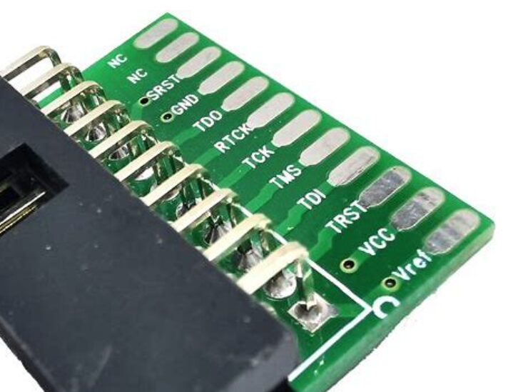
Pin Definition
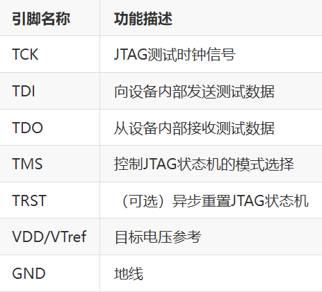
JTAG Pin Diagram:
SWD Interface
SWD (Serial Wire Debug) is a two-wire debugging protocol introduced by ARM, designed to provide a simple and efficient debugging interface for ARM Cortex series microcontrollers. SWD serves as an alternative to JTAG, using only two data lines instead of the four or five lines used by JTAG, and it is based on a bidirectional data protocol for data transmission and device control.
Main Features of SWD:
1. Fewer Lines: One of the biggest advantages of SWD is that it only requires two lines, which is very beneficial for miniaturized devices or designs with limited pins.
2. Efficient Data Transmission: Through optimized protocols and data encapsulation methods, SWD provides data transmission efficiency comparable to JTAG.
3. Simplified Protocol: The protocol design of SWD is relatively simple, making it easy to implement and debug.
4. Debug and System Trace: SWD not only supports debugging but can also be combined with technologies such as Serial Wire Viewer (SWV) and Serial Wire Output (SWO) to provide system-level tracing functionality.
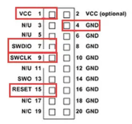
Pin Definition of SWD:
The SWD interface mainly includes the following pins:
1. SWCLK (Serial Wire Clock): This is the clock signal line used to synchronize data transmission.
2. SWDIO (Serial Wire Debug Data I/O): This is a bidirectional data line used for transmitting commands, addresses, and data.
These two lines replace JTAG’s TCK, TMS, TDI, and TDO.
Optional additional pins include:
1. nRESET (Optional): Used to perform a hardware reset on the target device.
2. SWO (Serial Wire Output, optional): Used for unidirectional communication, such as transmitting trace data from the target device to the host.
Working Principle of SWD:
SWD uses a 16-bit data packet for communication, with each data packet including an 8-bit header, followed by data and a parity bit:
Start Bit: The beginning of the data packet.
APnDP Bit: Distinguishes whether to access the Debug Port (DP) or the Access Port (AP).
RnW Bit: Indicates whether it is a read or write operation.
A[2:3] Bits: Two-bit address indicating which register of DP or AP is being accessed.
Parity Bit: Parity bit to ensure the integrity of the header information.
Stop Bit: The end of the data packet.
Park Bit: Fixed to 1 to ensure bus release.
Data transmission is synchronized by SWCLK, while SWDIO switches its direction as needed during read/write. In write operations, the host sends data on SWDIO, and the device replies with an ACK response in the subsequent clock cycle. In read operations, the device sends data back to the host on SWDIO after receiving the request.
Advantages of Using SWD:
1. Pin and Space Savings: Since only two lines are needed, SWD can save valuable PCB space and I/O resources of the microcontroller.
2. Debugging Efficiency: SWD provides fast debugging capabilities, including memory access and register operations.
3. Easier Routing: Compared to the multi-wire routing of JTAG interfaces, SWD simplifies the PCB design process by only considering the layout of two lines.
4. Real-time Tracing: Combined with SWO, SWD can achieve real-time data tracing and analysis, which is very useful for performance debugging.
Disadvantages:
1. Limited Chain Debugging: Unlike JTAG, SWD does not support chain connection of multiple devices and can only be used for a single target device.
2. Poor Universality: SWD is mainly designed for ARM processors, and other architectures may not support this interface.
Which One Should I Choose?
Since we are making an entry-level STM32 core board, considering the complexity and physical size limitations, we can confidently choose the SWD interface.
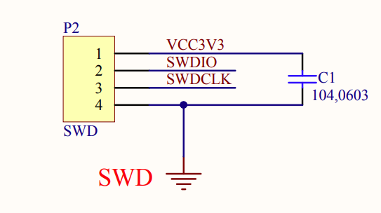
Circuit Analysis

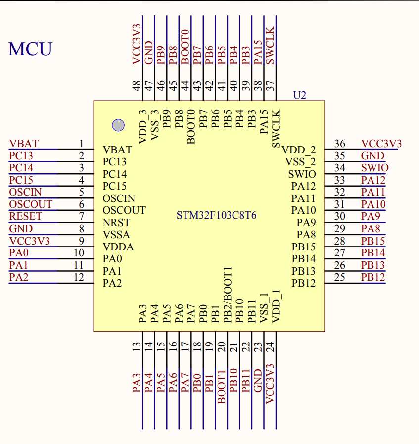
As we can see, SWD only uses four wires, greatly reducing the number of I/Os needed and simplifying the design of the download circuit. SWDIO and SWDCLK are connected to pins 34 and 37, respectively. The capacitor C1 here serves to decouple and smooth out instantaneous voltage fluctuations on the power supply line.