

NAND Flash is a type of non-volatile random access storage medium based on the design of floating gate transistors. It uses floating gates to store charges, which can be retained even without power supply. There has been a previous explanation of the basic principles of NAND Flash technology, which can be referenced in the article “The Most Comprehensive Analysis of Flash Memory Technology.” Today we will mainly discuss the production process, architecture, and key metrics of NAND Flash.
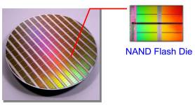
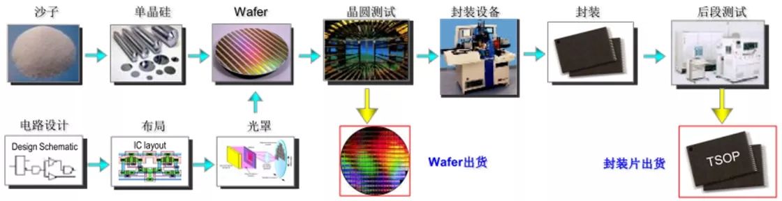
NAND Flash is processed from raw silicon material, which is fabricated into wafers. A single wafer can produce hundreds of NAND Flash chips. The unencapsulated chips are called dies, which are small pieces cut from the wafer using lasers. Each die is an independent functional chip composed of countless transistor circuits, but can ultimately be encapsulated as a unit to form a flash memory chip. Below is the detailed processing of NAND Flash chips.
The capacity structure of NAND Flash can be divided from large to small into Device, Target, LUN, Plane, Block, Page, Cell. A device has several dies (also called LUN), each die has several planes, each plane has several blocks, and each block has several pages, with each page corresponding to a wordline.
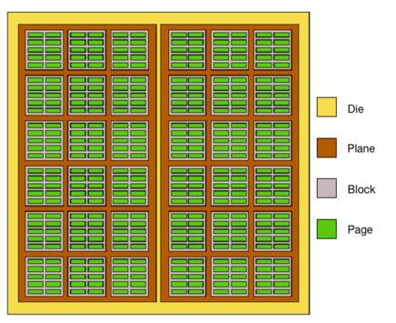
Die/LUN is the basic unit that receives and executes FLASH commands. Different LUNs can simultaneously receive and execute different commands. However, within a single LUN, only one command can be executed at a time; it cannot read from one page while writing to another page. Below is a detailed introduction to these structural units and their relationships.
-
A Device refers to a single NAND Flash chip that provides packaged chips to the outside, usually containing one or more targets;
-
Target has independently selectable units and can be addressed individually, usually containing one or more LUNs; LUN is the latest physical unit that can be independently packaged and usually contains multiple planes.
-
Plane has independent page registers, usually containing 1K or 2K odd or even blocks;
-
Block is the smallest unit that can perform erase operations, usually composed of multiple pages; Page is the smallest unit that can perform programming and read operations, typically sized at 4KB/8KB/16KB/32KB, etc.
-
Cell is the smallest operational erase-write-read unit in a page, corresponding to a floating gate transistor, capable of storing 1 bit or multiple bits of data, mainly in granule types.
The following diagram shows the organizational structure of a FLASH Block, where each cell’s drain corresponds to BL (Bitline), gate corresponds to WL (Wordline), and sources are all connected together. Each page corresponds to a wordline, and various operations are performed by applying different voltages and durations through the wordline.

A wordline corresponds to one or several pages; for SLC, one wordline corresponds to one page; for MLC, it corresponds to two pages (Lower Page and Upper Page); the size of the page corresponds to the number of storage units (cells) on the wordline.
Data Retention is a reliability metric used to measure how long the data written to NAND Flash can be retained without distortion. It is generally defined as the time data remains undistorted in NAND Flash under certain temperature conditions after using ECC (Error Correction Code). The two main factors affecting data retention are erase-write cycles and storage temperature. Typically, enterprise-grade SSDs follow the JEDEC JESD218 standard for data retention, which requires that at room temperature (40℃), after 100% PE cycles, the retention time must reach 3 months when powered off.
NAND Flash must be erased before writing; a block erased once and then written once is called one PE Cycle. Endurance is a reliability metric used to measure the write life of NAND Flash; it indicates the ability of NAND Flash to repeatedly erase and write data under certain test conditions, corresponding to NAND Flash’s PE (Program/Erase) cycle.
Bit Error Rate (BER) refers to the errors caused by the probability of bit flips in NAND Flash granules, where RBER (Raw Bit Error Rate) indicates the probability of a bit error occurring without ECC correction, and is also a metric for measuring NAND quality. RBER is a characteristic of NAND itself and worsens with increased PE cycles, exhibiting an exponential distribution of errors, mainly due to wear on the floating gate’s oxide layer caused by erase-write cycles.
UBER (Uncorrectable Bit Error Rate) indicates the probability of uncorrectable ECC errors, i.e., the likelihood that the number of bit flips in a codeword exceeds the correction capacity of the ECC algorithm.
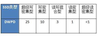
DWPD (Diskful Writes Per Day) refers to the amount of data written daily. The cost of SSDs ($/GB) increases with higher DWPD. The trend for future SSDs predicts that read-intensive workloads, which currently account for 50%, will gradually increase.
The lifespan of NAND Flash is not equal to the lifespan of SSDs; SSDs can use various technical means to enhance their overall lifespan. Depending on different technical means, the lifespan of SSDs can be improved by 20% to 2000% compared to the claimed lifespan of NAND Flash.

The lifespan of SSDs is not equal to that of NAND Flash. The lifespan of NAND Flash is primarily characterized by P/E cycles. SSDs are composed of multiple Flash granules, which can effectively utilize the lifespan of the granules through disk algorithms. Key factors affecting the lifespan of SSDs include:
-
Annual data write volume, closely related to the customer’s business scenarios;
-
Single Flash granule lifespan, as different granules have different P/E cycles;
-
Error correction algorithms, which extend the usable life of granules with stronger correction capabilities;
-
Wear leveling algorithms, which prevent uneven erase-write cycles from exceeding the lifespan of granules;
-
Over Provisioning (OP) ratio, as increasing OP (reserved space) can enhance the lifespan of SSDs.
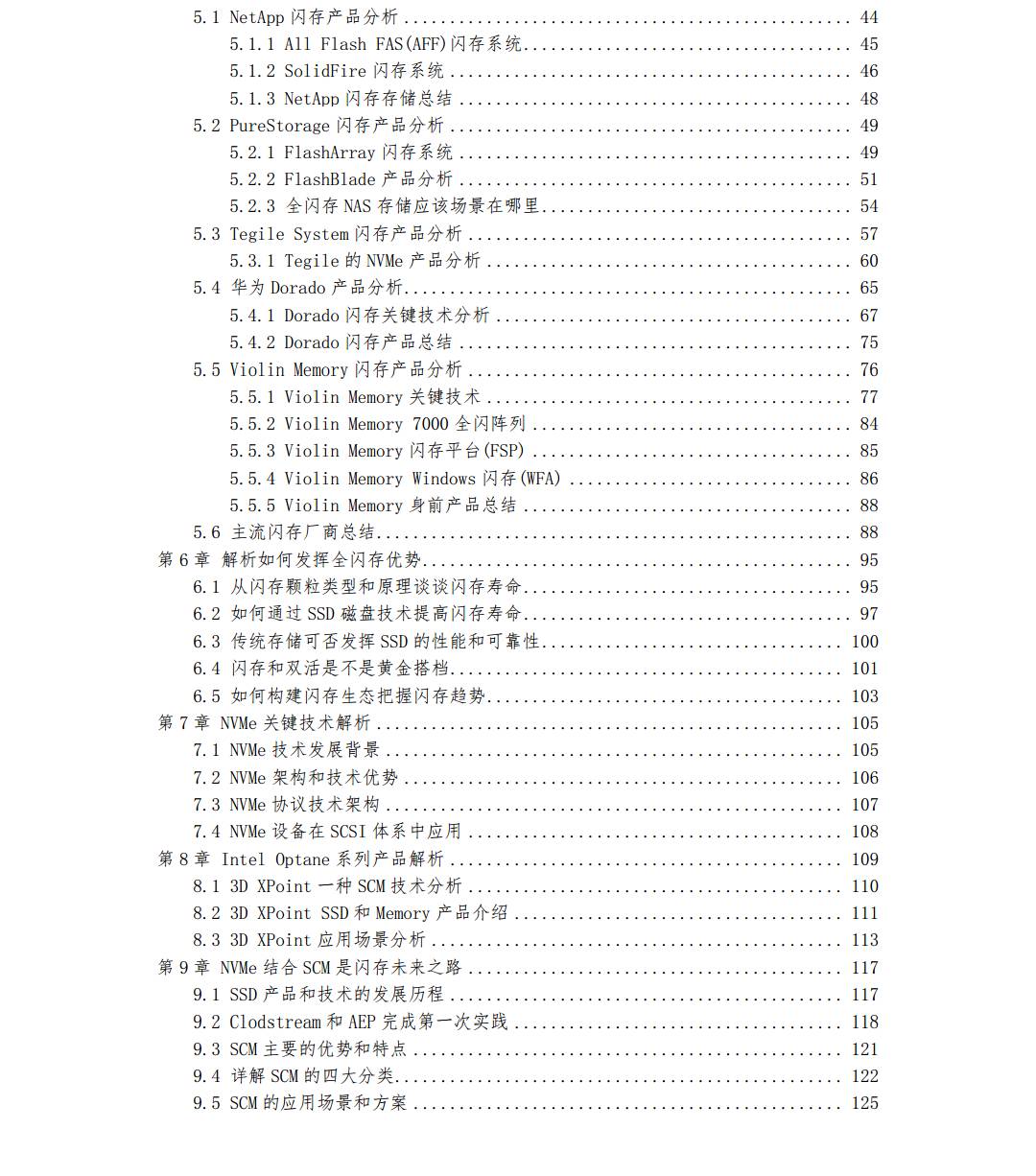
As professionals in flash memory development, design, and industry, it is essential to keep up with the times and follow the pace of new technologies. For further understanding of SSDs, flash memory, NVMe, and SCM technology, please refer to the “Comprehensive Analysis of Flash Memory Technology, Products, and Development Trends” materials, with the table of contents detailed below. 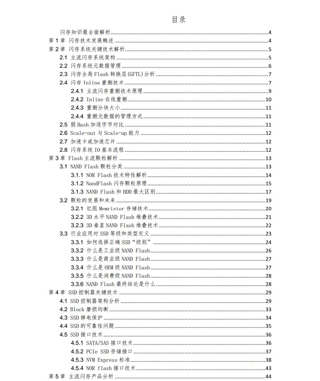
Click on the original link to view the most comprehensive “Analysis of Flash Memory Technology, Products, and Development Trends.”
>>> Recommended Reading
-
Analysis of the Evolution of High-Performance Computing (HPC) Technology, Solutions, Ecosystems, and Industry Development Trends
-
The Reference Value of This Article Behind the Storage Performance Bottleneck
-
How Distributed, Multi-active Data Centers Achieve DNS Domain Name Resolution and Load Balancing
-
What Remains Worth Remembering After the Traditional Enterprise Storage Battle
Warm Reminder: Please search for “ICT_Architect” or scan the QR code to follow the public account, and click on original link to obtain more technical materials.

Click on the original link to obtain technical materials