Abstract: A SAR imaging processing scheme based on multicore DSP interconnection architecture is proposed. First, a real-time imaging algorithm based on azimuth sub-block interpolation is introduced. Second, the processing performance of the TI multicore DSP TMS320C6678 is studied, and a typical RapidIO interconnection architecture is introduced, followed by the proposal of a SAR imaging processing scheme based on this architecture. Finally, the effectiveness and advancement of this processing scheme are demonstrated by providing SAR imaging results and comparing them with traditional solutions.
1 PFA Imaging Processing Algorithm
In the spotlight mode synthetic aperture radar, the antenna beam always points to a fixed imaging area, resulting in the radar’s rotation relative to the target area. The Polar Format Algorithm (PFA) was initially proposed as an effective method for imaging rotating targets and was soon successfully applied to spotlight mode SAR imaging, significantly improving the effective imaging range of spotlight SAR.
PFA is a classic spotlight SAR imaging algorithm that uses polar format to store data, effectively addressing the issue of moving resolution cells away from the center of the imaging area, greatly enhancing the effective focusing imaging range of spotlight SAR. Compared with other algorithms, the PFA algorithm has advantages such as simplicity, efficiency, low computational load, good real-time performance, and ease of motion compensation, making it widely used in the field of SAR real-time imaging.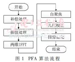
This paper adopts the PFA imaging algorithm, as shown in Figure 1.
The aforementioned PFA algorithm requires a large amount of data storage during interpolation processing, which increases storage capacity and also leads to increased imaging latency. The azimuth sub-block interpolation based PFA imaging algorithm divides the collection of all range lines into several overlapping subsets, with each subset treated as a sub-block, distributed to the corresponding processors for interpolation processing, reducing storage capacity requirements and lowering imaging latency.
2 TMS320C6678 Multicore DSP Processing Mode and Performance Study
2.1 Multicore DSP Processing Modes
TI has launched the new generation multicore DSP TMS320C6678 (C6678), which embeds 8 cores, with a maximum core speed of 1.25 GHz, and an industrial-grade chip can reach 1 GHz, with a single-core floating-point computing capability of up to 20 GFLOP. While the processing capability of C6678 has improved, it also has stronger IO capabilities, with RapidIO supporting up to 20 GB/s transmission and Ethernet supporting up to 1 GB/s transmission. The DSP’s memory is divided into local memory (LL2), shared memory (SL2), and external memory (DDR). Among them, LL2 is 512 KB, SL2 is 4 MB, and DDR can address 8 GB of space.
Common multicore processing modes include two types: master-slave mode and data flow mode, as shown in Figure 2.
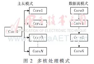
(1) Master-slave mode, where one core receives and distributes data, managing the processing of other cores, i.e., a 1+N working mode;
(2) Data flow mode, where processing is executed serially according to data transmission.
Due to shared data bandwidth among multicore processors, the data flow mode is only suitable for situations where the amount of data transferred between cores is small, while SAR processing involves large data volumes, thus the master-slave mode is adopted.
The multicore master-slave mode based on C6678 is shown in Figure 3. Since the cache occupies a portion of the LL2 storage space, the remaining capacity is small, so LL2 is only used for storing small amounts of constant data; SL2 is used to save intermediate results used by each core during processing; the DDR space is larger and can store a large amount of data needed for DSP input, output, and data rotation.
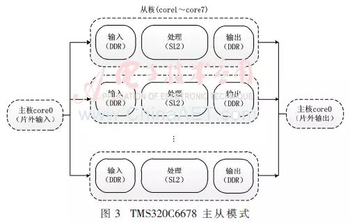
The master core first allocates the received DSP input data to the corresponding slave cores, then activates the slave cores for corresponding sub-processing based on different processing requirements, waits for all slave cores to finish processing, and finally aggregates the output results from the slave cores and sends them to other DSPs. This master-slave mode separates DSP processing from data transmission, simplifies the timing relationships between DSPs, and enhances system stability.
2.2 Multicore DSP Processing Performance Study
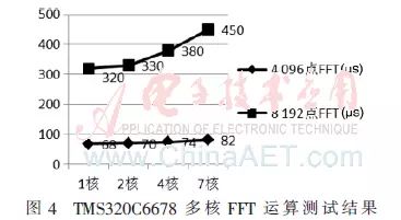
Based on the aforementioned master-slave mode, using FFT computation as an example, the parallel processing performance of the C6678 multicore is tested. As shown in Figure 4, as the number of parallel cores increases, the FFT processing time also increases, which is due to the shared SL2 data bandwidth among multicore processors, leading to competition during parallel processing of slave cores, thus decreasing the DSP’s parallel processing capability. Therefore, the multicore parallel processing capability does not increase linearly with the number of participating slave cores.
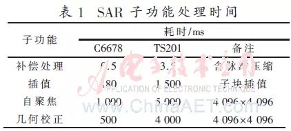
Based on the PFA imaging algorithm process, using the 1+4 master-slave mode (1 master core plus 4 slave cores) as an example, the multicore parallel processing performance of various sub-functions in SAR processing is tested and compared with the single-core DSP TS201, with results shown in Table 1. Due to differences in the main frequency, memory bus width, optimization capability, etc., between the two processors, and because certain sub-functions are not suitable for parallel processing (such as the self-focusing iterative process), the processing capability of C6678 is not simply a 4-fold relationship to that of TS201.
2.3 Maintaining Cache Coherency
The results provided above are based on the premise that cache is enabled in the DSP. For C6678, each core can allocate cache space in LL2, and with cache enabled, each core’s read and write operations on SL2 are performed in the cache, greatly improving memory read and write efficiency. For example, in the case of 4096-point FFT computation, the time taken with cache enabled is 68 μs, while it reaches as high as 600 μs without cache enabled.
However, enabling cache can lead to cache coherency issues, which refer to the inconsistencies caused by multiple copies of data in parallel systems with multiple caches not being synchronized. Software is needed to maintain cache coherency, with operations divided into cache invalidation and cache write-back. For instance, when core A needs to update data for core B, core A must first perform a cache write-back operation to update the data in the cache to memory, and core B must perform a cache invalidation operation before reading the updated data from core A to ensure that the data read from the cache is consistent with that in memory. In addition to maintaining cache coherency between multicore processors, it is also necessary to maintain cache coherency between cores and peripherals (such as SRIO, EDMA, etc.) since peripheral read and write operations do not go through the cache.
3 Design of a Real-Time Processing System for SAR Based on RapidIO Interconnection
Enhancing the processing capability of the DSP is only one aspect of ensuring system real-time performance; in typical embedded systems, the bottleneck often lies in the system-level interconnection, i.e., the communication speed between components. The RapidIO interconnection architecture eliminates this bottleneck, providing a high-performance, packet-switched interconnection technology. Currently, C6678 supports transmission rates of up to 20 GB/s.
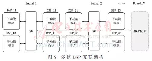
Figure 5 shows a typical multicore DSP interconnection architecture, where board-level DSPs are interconnected through switching devices (SW), and inter-board connections are also made through SW, forming a RapidIO interconnection network. Traditional fixed topology architectures make each DSP in the system irreplaceable due to a single communication link. In contrast, in this interconnection architecture, the logical positions of DSPs in the system are equivalent, allowing for easy system reconfiguration. Moreover, this interconnection architecture uses 4 DSP boards as the minimum unit and can be expanded according to system requirements. This RapidIO interconnection architecture allows software design to no longer be limited by fixed topologies, offering high reconfigurability and scalability.
To fully utilize the parallel processing capabilities of multicore DSPs, each sub-function module needs to complete as many functions as possible, which also reduces data transmission between sub-function modules and thus reduces pipeline stages, lowering system complexity.
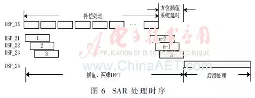
The timing of SAR processing is shown in Figure 6, where compensation processing, due to high real-time requirements, requires 4 DSPs for rotating processing, with the processing results also rotated and sent to DSP_21, DSP_22, and DSP_23 for sub-block interpolation and two-dimensional IFFT processing. After DSP_21, DSP_22, and DSP_23 complete their processing, they send the output results to DSP_24, which generates the complex image for subsequent processing after receiving all sub-block results, ultimately producing and outputting the image.
4 Imaging Result Verification
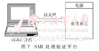
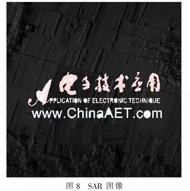
Figure 7 shows the verification platform for the SAR imaging processing system, where the debugging computer inputs raw data obtained from test flights via Ethernet, which undergoes SAR imaging processing through the processing system, with the imaging results shown in Figure 8, achieving an image resolution of 0.5 m. As can be seen from the figure, the image is well-focused, with clear details and rich layers, verifying the effectiveness of the imaging system.
Traditional single-core DSP architectures require as many as 40 DSPs to barely ensure real-time SAR imaging processing, while this multicore DSP architecture only requires 8 DSPs to meet the demand, with still some margin left (each DSP only uses 5 cores), highlighting the significant advantages of this multicore DSP interconnection architecture.
5 Conclusion
This paper presents a real-time SAR imaging processing algorithm suitable for engineering implementation, focusing on the processing modes and performance of multicore DSP (C6678), and provides a detailed analysis of the cache coherency issues in multicore DSPs. Based on the research conclusions, the sub-function modules of SAR processing were tested and verified. Subsequently, a typical RapidIO interconnection architecture was introduced, and a SAR imaging processing system based on this architecture was designed and implemented. The results indicate that this system has advantages in efficiency, reconfigurability, and scalability compared to traditional architectures.