
DAP and JTAG
There are various ways to connect to the Debug Access Port (DAP), which differ in cost, invasiveness, and security. The DAP allows access to the core within the chip, which is typically the first to boot or is a dedicated microprocessor used for managing chip boot, debugging, and initializing DVFS and DRAM configurations. Since the debug channel provides a backdoor to access the chip, some security measures need to be implemented to protect against reverse engineering and malicious programs, preventing theft of chip intellectual property and data. Common practices include:
-
Physically connecting dedicated pins on the chip directly to unused sockets on the circuit board;
-
Using encryption and secure boot mechanisms;
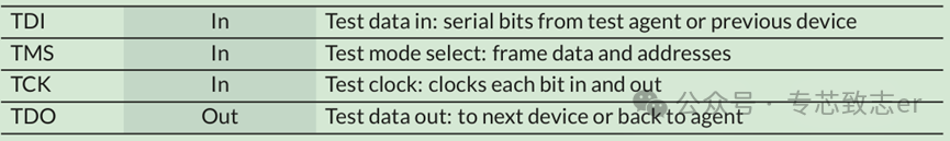
The most widely used and oldest method in DAP is JTAG (Joint Test Action Group). JTAG is a serial bus used for testing registers within the chip, originally intended for boundary scan testing of board-level products, and consists of four pins:
Table 1 JTAG Pins
Typically, a circuit board will have many chips with DAP ports, which are connected in a daisy chain, as shown in Figure 1. In a daisy chain, there can be any number of chips and any length of registers. These test registers provide a bypass register for accessing the next chip in the chain. During the JTAG testing process, the value on the TMS pin can address any test register value in any chip within the daisy chain. Similar to the function of a shift register, the old values of the test registers are shifted out, and new values are shifted in. Of course, for RO registers, the new values will be ignored. Certain predefined registers are used to store manufacturer and device IDs, allowing the debugger software to dynamically adjust the physical order and presence of different chips on the board.
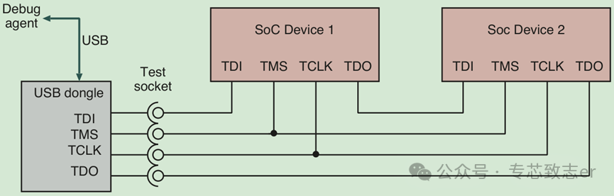
Figure 1 JTAG Daisy Chain on the Board
The access speed of JTAG is typically limited to a few Mbps, so other higher-performance parallel interfaces like USB are used for DAP ports that require faster speeds.
The DAP port is also used for other chip-level testing and manufacturing, such as:
-
Hiding (degrading) some defective products to lower specifications or replacing them with other redundant components;
-
Calibrating ring oscillators and DVFS;
-
Installing MAC addresses, PKI keys, or other data that need to be generated across different SoCs;
-
Refreshing BIOS and file systems;
-
Accessing built-in self-test (BIST) mechanisms;
Boundary Scan
After chip manufacturing, boundary and general path scanning are typically performed on the chip, with Figure 2 showing a segment of the boundary scan path. To support boundary scanning, some basic logic circuits are added to the input and output pads. Serial data is shifted from one pad to another under the control of a test clock. As test vectors are shifted in, the results of previous test vectors are shifted out. Two Strobe signals are used to inject test vectors into the input pads and sample data on the output pads.
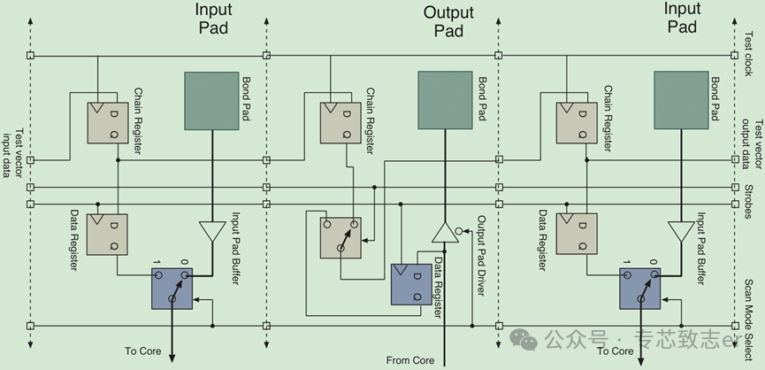
Figure 2 Boundary Scan Path
When the scan mode select is low, the scanning logic does not affect the normal operation of the chip. Conversely, when the scan mode is activated, the boundary scan logic takes over the input pads, using shift and store methods for testing. To support scanning, two new registers are added to each pad: the Chain Register and the Data Register. The chain register is used for data transfer in the scan chain, with the measurement vector length required for shifting from the DAP controller equal to the number of test pads. Strobe signals can be used to capture data from the output pads and inject new data into the input pads. As the next test vector data is shifted in, the captured data will be shifted out bit by bit. The data register primarily ensures that the test vectors already used remain stable during the shifting process in the scan chain.
Boundary scan can be applied to IP blocks and hard macro units within the chip, such as custom processor cores. However, with the standardization of on-chip buses, such as the AXI standard bus, boundary scanning of IP modules has become less common. The currently used BIST scanning is similar to boundary scanning, but it scans paths through all internal flip-flops of the IP, allowing observation of data for each cycle of the component, but it prevents the component from running at full speed while being scanned and adds significant wiring overhead. Generally, the logic for universal scan paths can be inserted by logic synthesis tools in special modes.