JTAG: The Core Interface for Chip Testability Design
In the field of integrated circuit (IC) design, Design for Testability (DFT) is a key technology to ensure high reliability and yield in chip production. JTAG (Joint Test Action Group), as a standard test access interface, has become an important means for modern chips to implement DFT functions.
As the core technology of the IEEE 1149.1 standard, JTAG is a critical component of integrated circuit testability design (DFT). Its original goal was to address the challenges of testing high-density PCB (Printed Circuit Board) interconnections, and it has now become the testing standard for the entire lifecycle of chip design, production debugging, and field maintenance. Through JTAG technology, engineers can efficiently test and control the state of chip pins, internal logic, and system-level interconnections without relying on physical probes.
1. JTAG Basics: A Standardized Test Interface
1. History and Standards of JTAG
Origin: Established by the JTAG consortium in 1985, it became the IEEE 1149.1 standard in 1990.
Goal: To solve the challenges of board-level interconnection testing for high-density PCBs, later expanded to chip-level testing and debugging.
Core Functions:
Pin state control and observation (Boundary Scan).
Access to internal chip registers (such as debug registers).
Programming and configuration (such as JTAG programming for CPUs/FPGA).
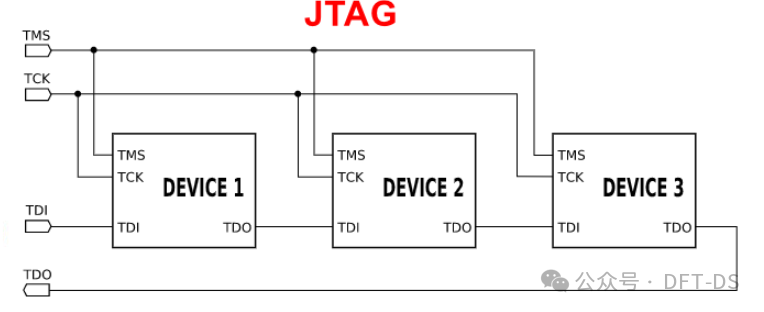
2. Hardware Architecture of the JTAG Interface
The JTAG interface includes the following key components:
1) TAP (Test Access Port) Controller:
A state machine driven by TCK (Test Clock) and TMS (Test Mode Select) signals, controlling the test process.
The state transition diagram includes states such as Run-Test/Idle, Capture-DR, Shift-DR, Update-DR, etc.
2) Instruction Register (IR) and Data Register (DR):
IR: Stores the current operation instruction (such as EXTEST, BYPASS).
DR: Includes Boundary Scan Register (BSR), BYPASS register, etc., for data transfer.
3) Boundary Scan Cell (BSC)
Each chip pin is connected to a BSC, supporting input capture, output driving, and signal isolation.
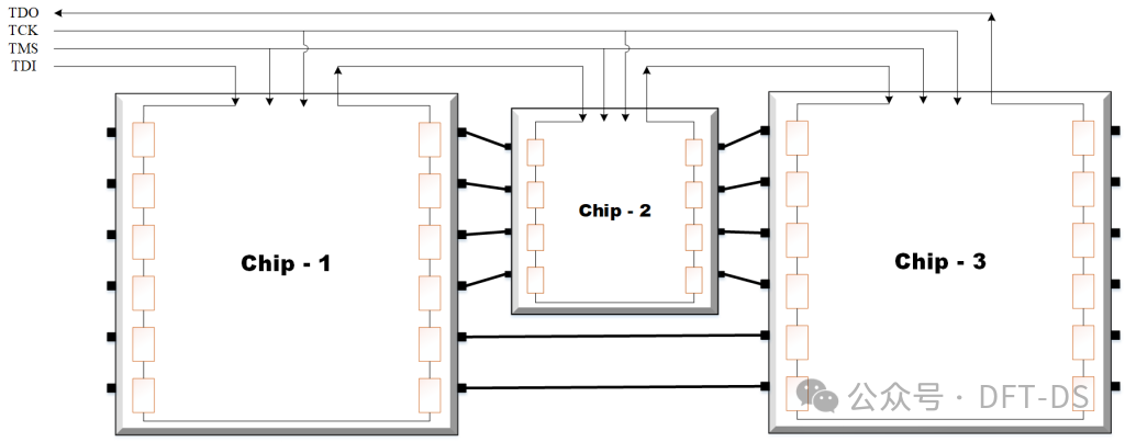
Multiple JTAG interconnections form a boundary scan chain to achieve board-level interconnection testing.
2. Collaborative Design of JTAG and DFT
1. Design Process
Architecture Planning: Determine the length of the scan chain and the topology of the JTAG chain (single chain or multi-chain), optimizing test efficiency.
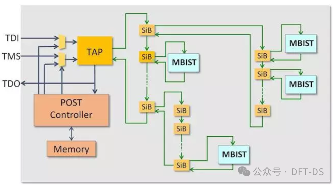
RTL Integration: Insert TAP controller and boundary scan units, ensuring compatibility with other IP cores (such as FPGA, CPU) interfaces. Use existing or inserted JTAG interfaces to control DFT-related signals, such as test modes, IP configurations, etc. JTAG can also serve as input signals for DFT logic like MBIST, used for DFT pattern input and result observation.
Physical Implementation: Optimize the layout of the scan chain, reduce signal delay, and ensure timing convergence.
Verification and Debugging: Locate faults through Logic Equivalence Checking (LEC) and post-silicon JTAG interface.
2. Application Scenarios of JTAG
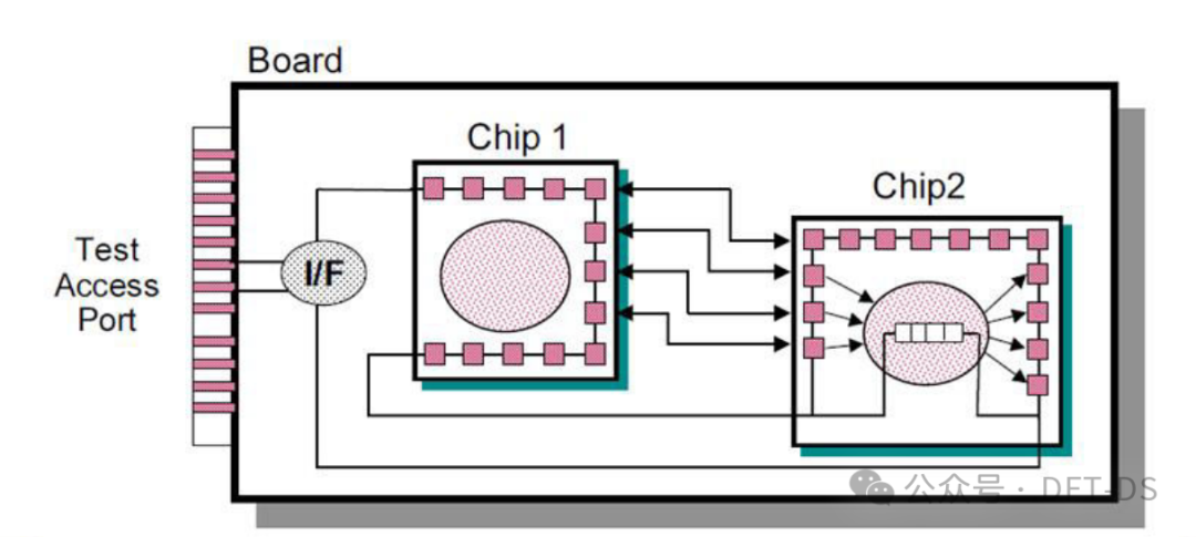
1). Board-Level Interconnection Testing
Problem: Difficulties in locating shorts and opens between chips on the PCB.
Solution:
Load test vectors into the BSC (Boundary Scan Cell) of the driving chip via JTAG.
Capture the input signals of the receiving chip to verify if the electrical connections are correct.
Advantage: No physical probes are needed, supporting high-density, miniaturized PCB testing.
2). Internal Logic Testing of Chips
Scan Chain Integration: Combine JTAG with internal scan chains to achieve the following process:
Shift-In: Shift test vectors into the scan chain via TDI (Test Data Input).
Capture: Apply clock to capture circuit responses.
Shift-Out: Shift out responses via TDO (Test Data Output) and compare with expected results.
Case: Logic fault detection in CPU cores.
3). Online Debugging and Tracing
Real-time Access: Read internal registers and memory contents of the chip via JTAG.
Debugging Functions: Set breakpoints and watchpoints. Trace program execution flow.
Application Scenario: Fault diagnosis in embedded systems (such as automotive ECUs).
4. Chip Configuration and Programming
FPGA/CPU Configuration: Download bitstream files via JTAG.
Flash Programming: Program bootloaders or firmware (such as ARM Cortex-M series MCUs).
3. Advantages and Challenges of JTAG
1. Core Advantages
Standardized Interface: Strong compatibility with IEEE 1149.1, mature toolchains (such as OpenOCD, Segger J-Link).
Non-Intrusive Testing: No need to damage chip packaging or PCB structure.
Multi-Functional Integration: One-stop solution for testing, debugging, and programming.
2. Challenges Faced
Speed Limitations: JTAG clock frequency is usually below 10 MHz, making it difficult to meet high-speed testing requirements.
Area and Timing: JTAG logic and boundary scan chains increase chip area (about 1%~5%) and may affect the timing of high-speed signals.
Security Risks: JTAG interfaces may become hardware backdoors, requiring protection through fuses or encryption.
4. Future Development Trends of JTAG
1. High-Speed and Protocol Expansion
IEEE 1149.7: Supports multi-TAP cascading and high-speed transmission modes.
cJTAG (Compact JTAG): Reduces pin count to meet miniaturization packaging needs.
2. Integration with AI Chips
Intelligent Debugging: Real-time collection of operational data from AI accelerators via JTAG to optimize model performance.
Dynamic Reconfiguration: Adjust neural network parameters at runtime.
3. Automotive Electronics and Functional Safety
ISO 26262 Compliance: JTAG is used to verify fault injection and fault tolerance mechanisms in chips.
OTA Upgrades: Remote updates of onboard firmware via JTAG interfaces.
As the core interface of DFT technology, JTAG not only solves the physical access challenges of traditional testing but also greatly enhances the observability and controllability of chips. With the continuous increase in the complexity of integrated circuits, the value of JTAG in testing, debugging, and security will become even more prominent.