1. Soldering of PoP
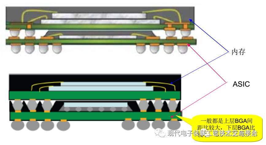
1.2 Process Methods
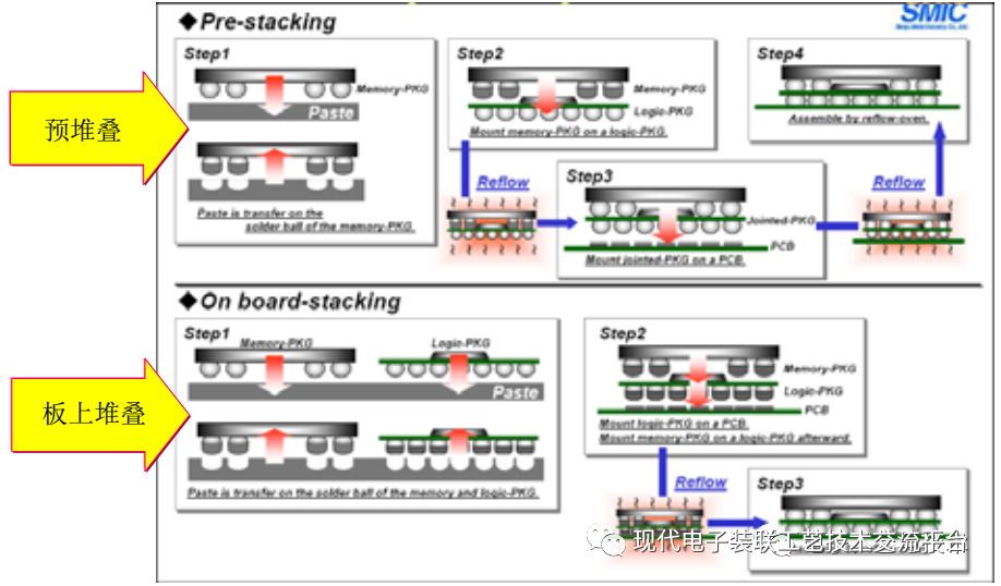
The production mainly adopts the on-board stacking process, which has two methods:
1) Solder paste method; 2) Solder paste method.
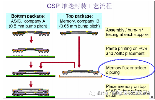
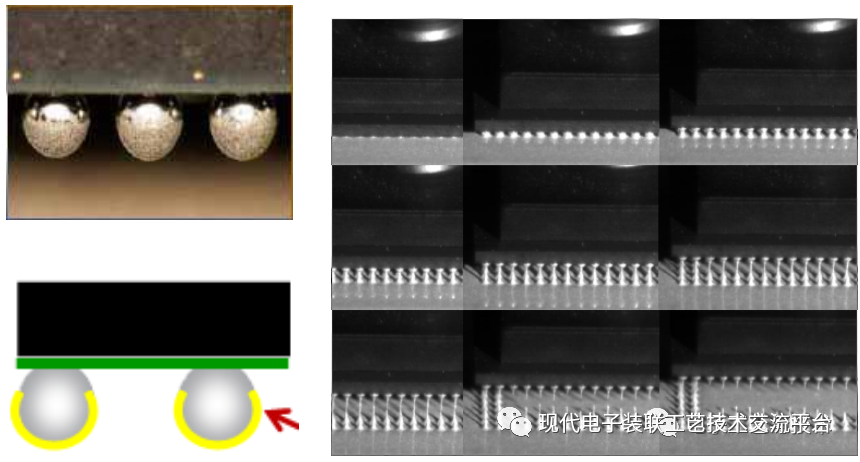
The core of the process: The process of applying flux or solder paste.
1.3 Common Soldering Defects
1) Open solder/ball pit
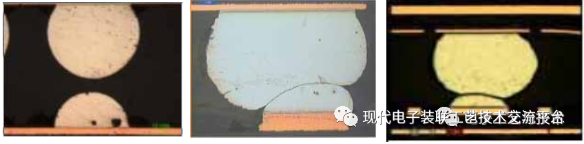
1) Bridging
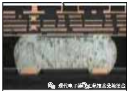
1.4 Mechanism and Causes of PoP Ball Pits
1) The mechanism is similar to the BGA ball pit phenomenon, but more complex, with the interaction of two layers.
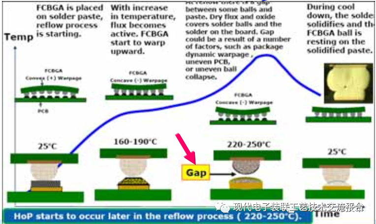
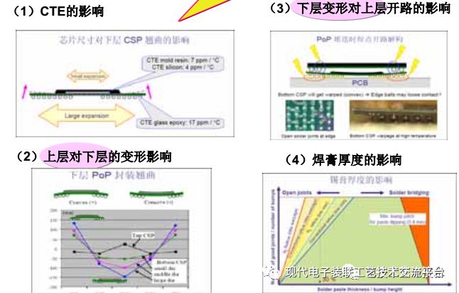
The mechanism: There is a gap between the molten solder ball and the molten solder paste! The reason for the gap is BGA deformation. The thinner the BGA, the easier it is to deform, with F-BGA and P-BGA being the most severe.
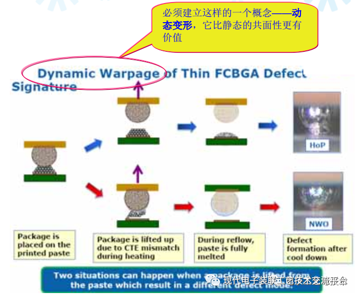
2) Main Causes of PoP Deformation
In addition to BGA deformation factors, PoP ball pits also involve mutual influences between upper and lower layers.
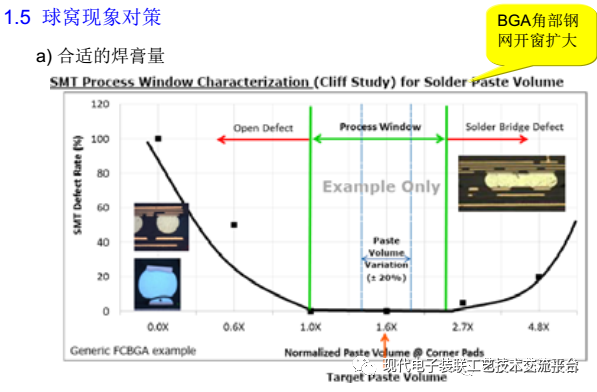
b) Improve the positioning accuracy of the chip;
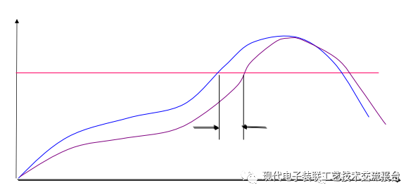
c) Optimize the temperature curve to reduce the time of different melting.
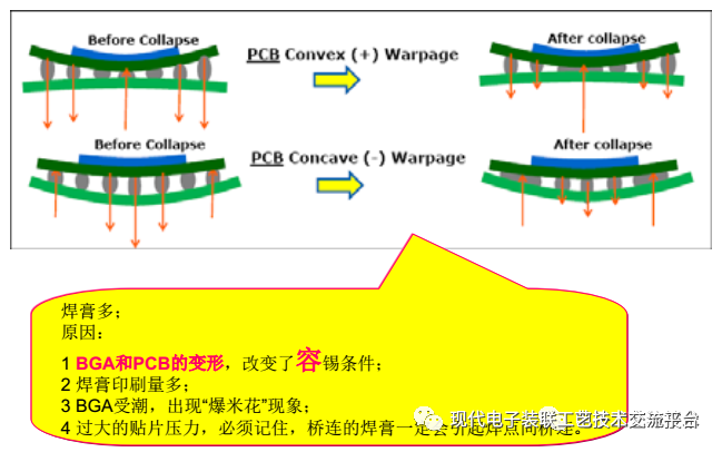
1.6 Causes and Countermeasures of Bridging Phenomenon
1.7 Special PoP Case——ML PoP
1) What is ML-PoP?
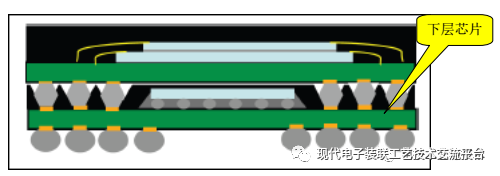
ML-PoP, or Molded Laser PoP, is a type of “ball pit” pad packaging form invented by Qualcomm, as shown in the POP below. Compared to flat pad PoP, MLP is more prone to ball pits and bridging phenomena. The packaging quality and process conditions greatly affect the soldering yield.
2) Core of the Process
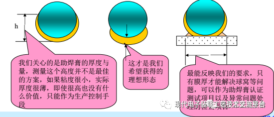
Requirements for Solder Paste Thickness
The thickness of solder paste applied to the upper chip solder balls should be as much as possible, but it must not cover the bottom of the chip package. More thickness improves the chip’s self-alignment capability, resulting in round and full solder joint shapes during X-Ray inspection; less thickness reduces the chip’s self-alignment capability, leading to a higher probability of oval solder joints due to the offset of the upper and lower balls.
Production Control Requirements: Generally h≈50~70%, 60% is optimal.
3) Solutions to Production Problems
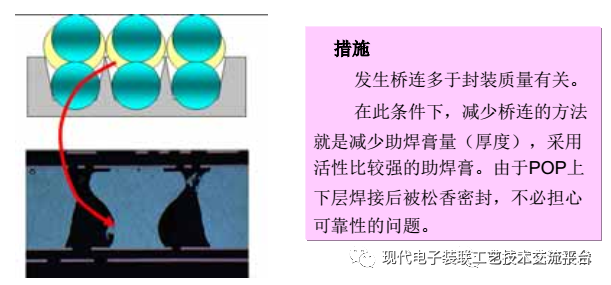
(1) Bridging
The cause and mechanism are that due to the deep laser pit, excessive flux will seal the pit, forming a closed air space. When heated, the gas expands and pushes the molten solder out, resulting in bridging!
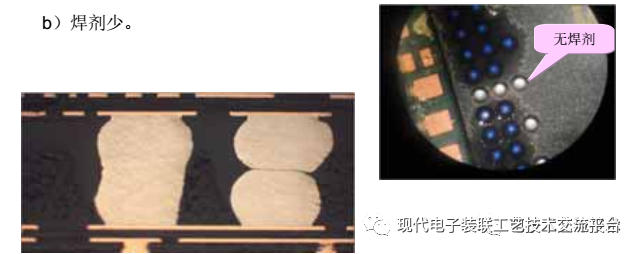
(2) Ball Pits
Causes: a) Insufficient temperature, resulting in double ball shapes at the solder joints.
2. Soldering of QFN
2.1 QFN
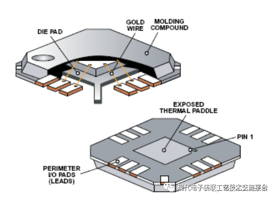
QFN belongs to the earliest and most widely used type of bottom solder pad packaging in the BTC packaging category, characterized by the solder pads being embedded within the package body, as shown in the figure.
2.2 Process Characteristics
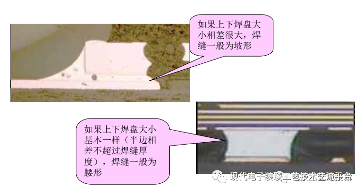
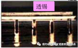
1) The solder pads of QFN are essentially a surface (0~0.05mm), forming a “surface-surface” connection with the PCB pads. The normal solder joint morphology is shown in the figure, where the non-edge side solder joints are either “waist” or “slope” shaped, and generally do not form the “bulge” shape like BGA, which is very beneficial for eliminating bridging defects under the QFN package.
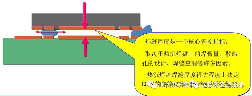
2) Due to the almost “0” bottom (Stand-off) gap and large size of thermal pad solder pads, the QFN process is quite complex. Compared to other packages, it is essential to consider the balance of the solder joint thickness between thermal pads and signal pads!
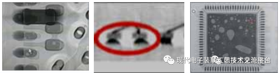
3) The most common soldering issues are bridging and cold solder joints, as well as exceeding the void standard of thermal pad solder joints, as shown in the figure. Bridging mainly occurs when the Cu spacing is less than 0.25mm. Cold solder joints often result from reducing the opening of the stencil to minimize bridging. The exceeding void standard of thermal pad solder joints is related to multiple factors and is fundamentally a comprehensive issue determined by PCB thickness, surface treatment, thermal hole diameter, density, solder mask, solder paste, and stencil opening.
4) Reliability of solder joints
The reliability of QFN solder joints mainly depends on the design of QFN. Generally, the larger the pad spacing, the better; the smaller the die area, the better; the smaller the QFN package size, the better; the thinner the PCB, the better.
2.3 Bridging Phenomenon, Causes, and Countermeasures
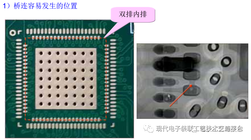
2.3 Bridging Phenomenon, Causes, and Countermeasures
2) Main Causes
Insufficient solder volume on thermal pad solder joints.
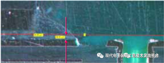
The solder joint thickness that can be formed on thermal pads is relatively smaller than that of signal pads due to coverage and thermal hole absorption (without plugged holes), and under surface tension, the solder on the surrounding signal pads is squeezed and expanded, easily causing new bridging phenomena.
[Experiment]
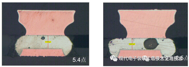
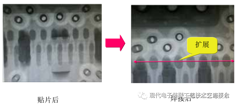
The effect of thermal pad solder paste volume on the solder joint morphology of QFN signal pads:
Using printing technology, the solder paste volume on signal pads remains unchanged (two printing points in the inner circle), while the thermal pad solder paste volume is one 5.4 and one 2.5, resulting in the soldering outcome. This indicates that the amount of solder paste on thermal pads significantly affects the solder joint morphology of surrounding signal pads! Because the solder joint thickness determines the size of solder expansion (QFN solder joints do not have Z-direction wetting).
b) Use a thick stencil, such as 0.127mm (5mil).
c) Use a small stencil opening.
Since QFN pads are relatively small, mostly between 0.2~0.255×0.4~0.45, reducing the stencil opening easily brings the risk of cold solder joints. If the stencil thickness is reduced, it will counteract the effect of reducing solder paste volume due to the smaller opening and lead to reliability issues.
d) Use a thin solder mask design, avoiding layout vias and silkscreen characters near QFN pads.
2.5 Void Phenomenon, Causes, and Countermeasures
1) Main Causes
a) Large area of thermal pad.
b) Related to the design of thermal pad holes, especially whether the holes are plugged.
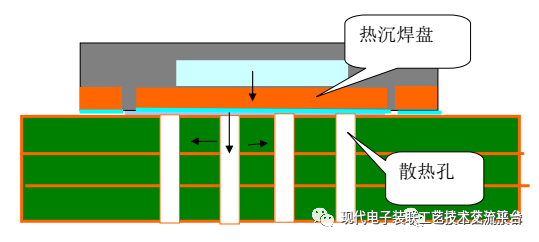
Thermal pads are designed for heat dissipation, and heat dissipation is achieved by conducting heat to the ground layer through thermal holes, as shown in the figure.
Thus, thermal pads generally have many holes. To prevent solder from leaking through the thermal holes during soldering, semi-plugging treatment is often applied, which is the main reason for large voids.
2) Countermeasures
(1) Design without plugging thermal holes
To reduce the occurrence of large voids in thermal pad solder joints, do not plug the thermal holes. Under these conditions, the following methods can generally be used to reduce solder leakage:
a) Place QFN layout on the surface for the second soldering; even if solder leaks, it will not affect the assembly process;
b) For larger thermal pads, use larger diameter thermal holes, such as 0.5~1.0mm;
c) Use small hole designs while maintaining sufficient wall spacing for easy application of solder paste printing technology; d) Design the PCB surface treatment as OSP;
e) Increase the PCB thickness to above 2.0mm; f) Place holes around the thermal pad.
(2) Optimize stencil opening design
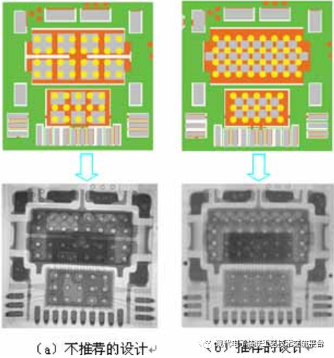
a) Do not include thermal holes in the solder paste pattern; design solder mask strips to establish venting channels.
3. BGA Voids
3.1 Types of BGA Voids
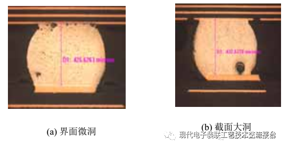
BGA voids, as shown in the figure, can be simply divided into two categories based on their occurrence location and size:
(1) Interface micro-voids: Small voids, numerous, appearing at the interface between the BGA side IMC and solder balls, as shown on the left.
(2) Large section voids: Single voids appearing inside BGA solder balls, as shown on the right.
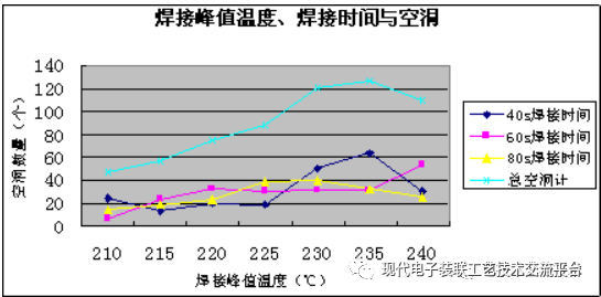
3.2 General Causes
(1) Flux system, mainly due to deficiencies in the flux formulation (external factor);
(2) Severe oxidation of BGA solder ball surfaces (internal factor);
(3) Inappropriate relative amounts of solder balls and solder paste (external factor).
(4) Use of N2 atmosphere during soldering. In practice, we found that voids in solder paste under N2 atmosphere conditions are more severe, as N2 reduces the surface tension of molten solder balls.
(5) The occurrence of voids is not greatly related to temperature curves or BGA moisture absorption; they only affect the number of voids.
3.3 Mechanism Speculation
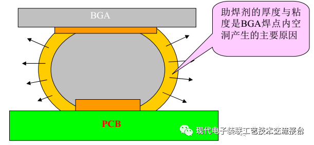
Under what circumstances does the flux have a higher viscosity or more volatiles? Generally, there are the following situations:
(1) The solvent boiling point in the flux system is relatively low. If the solvent boiling point in the flux is low, the flux will be more viscous when the solder paste is in a molten state. This is why lead-free solder paste results in fewer voids in lead-free BGA.
(2) Severe oxidation of solder balls. The thicker the oxidation layer on solder balls, the more metal salts generated by the flux reaction, which increases the viscosity of the flux. This is why some brands of BGA are prone to voids while others are not.
(3) The smaller the solder ball size, the more likely voids are to occur under the same amount of solder paste. This is because smaller solder balls have thicker coatings of flux, making it more difficult for volatile substances to escape.
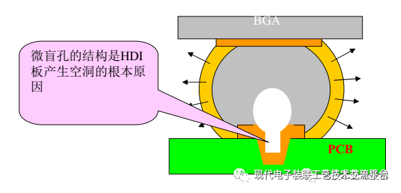
For HDI boards, in addition to the above reasons, the main factor is the structure of micro-blind holes on the pads. Micro-blind holes often contain many organic residues, and their volatiles are the main factors forming BGA voids on HDI boards, as shown in the figure.
3.4 Countermeasures
(1) Switch to suitable solder paste or other brands of BGA;
(2) Switch to active solder paste;
(3) Reduce the amount of solder paste;
(4) Design pad sizes according to solder ball sizes.
4. BGA Ball Pits
4.1 Ball Pit Phenomenon
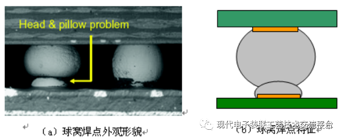
The solder ball does not connect with the solder paste, forming a ball pit on the solder ball side, as shown in the figure. This defect belongs to a type of cold solder joint and often occurs under lead-free processes and micro pad conditions.
4.2 Causes
There are many reasons, mainly two aspects:
(1) Deep oxidation of solder ball surfaces;
(2) During soldering, the solder ball and solder paste did not contact during the first collapse, such as BGA deformation or thin solder paste, the mechanism is shown in the figure.
(3) Large offset in placement can also lead to the ball pit phenomenon, similar to the mechanism of poor coplanarity leading to ball pits.
5. BGA Stress Fracture
5.1 Characteristics of Stress Fractures
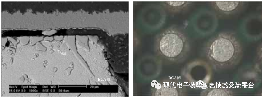
BGA solder joint stress fractures generally occur at the BGA side IMC and pad interface, with typical features showing a sandy fracture surface, as shown in the figure.
5.2 Cause Analysis
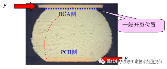
The stresses acting on the solder joint can be either mechanical stress or thermal stress. Mechanical stress refers to the stress generated by the interaction among various parts of an object when it deforms due to external forces. Thermal stress refers to the stress generated when the temperature changes, as the object cannot freely expand or contract due to external constraints and internal mutual constraints. The stresses they generate are different; generally, mechanical stress is tensile stress, while thermal stress is compressive stress. However, regardless of the type of stress, the destruction mechanism of the solder joint is the same, that is, the shear stress acting on the solder joint exceeds the capacity that the solder joint can withstand, leading to a break, as shown in the figure.
Lead solder joints contain only tin and lead alloy phases (solid solution), and the solder joint is in a soft state, as shown in the left figure. If the solder joint is subjected to stress, it generally absorbs it directly.
Lead-free solder joints increase the yield strength of the solder joint but reduce plasticity, as shown in the right figure. When the solder joint is subjected to stress, it cannot absorb it and is directly transmitted to the IMC layer, making IMC a key factor affecting reliability.
5.3 Countermeasures
To reduce the probability of stress fractures, on one hand, standardize operations to reduce stress; on the other hand, improve the strength of solder joints to avoid excessive IMC growth.
1. Strictly control soldering temperature and time
Cu’s solubility in molten SAC305 is 8.6 times that in Sn63/Pb37, and when reacting with SAC, it forms a thicker IMC layer. This is different from the lead process, where the IMC formed by Cu and SnPb solder generally does not exceed 2.5μm due to the inhibiting effect of Pb, but under lead-free processes, the IMC thickness formed by Cu and SAC305 can easily exceed 10μm. An effective measure is to minimize the duration of liquid BGA solder balls to avoid prolonged IMC growth.
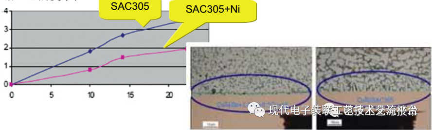
2) Use low Ag + Ni alloys
Low Ag + Ni alloys have excellent mechanical vibration resistance. Ag is an element that accelerates the growth of interface IMC,
Ni inhibits the production of Cu3Sn, as shown in the left figure.
For example, the reaction of Cu with Sn + 1.2Ag + 0.5Cu + Ni solder alloy forms a thin and flat IMC. At 250°C, only a 2μm thick IMC layer is formed. Low Ag with Ni has the effect of preventing IMC growth, as shown in the right figure. It also indicates that the IMC composition and morphology formed by Cu with different lead-free solders are different, reflecting the complexity of lead-free processes!
3) Assembly using tooling
Especially for screw assembly operations, if no base tooling is used, each time a screw is installed, the PCB will bend. If there are multiple screws on the PCB, multiple bends will occur, which can be very damaging to BGA.
6. Cracking and Operation of Chip Capacitors
6.2 Typical Failure Characteristics
1) Crack characteristics under mechanical stress
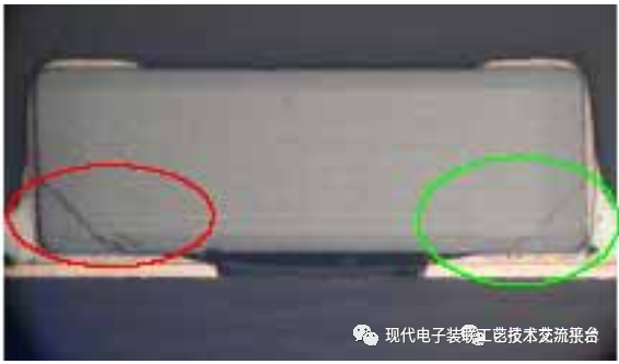
Cracking caused by mechanical stress has very typical features, generally located under the solder joint, with a 45° angle crack, as shown in the figure. This type of crack is generally not visible externally and is difficult to inspect.
2) Crack characteristics under thermal stress
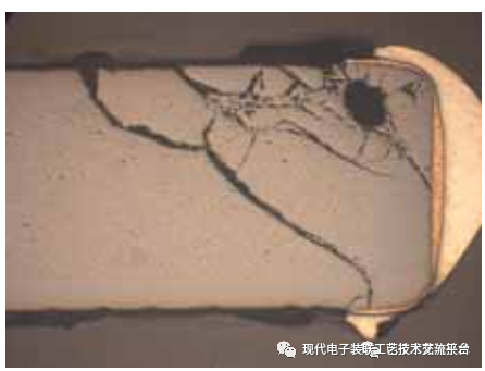
Ceramic chip capacitors, if internal voids exist, are prone to leakage. Leakage can cause temperature rise, which in turn exacerbates leakage. Under repeated cycling, thermal explosions can occur, forming branch-like cracks, as shown in the figure. This type of explosion is caused by thermal stress, so we classify it as thermal stress cracking.
6.3 Typical Cases
Case 1: Local thermal stress causing chip capacitor cracking
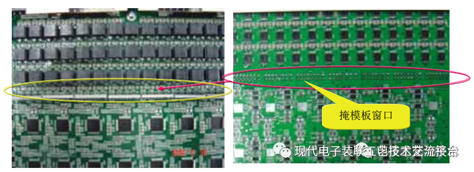
In a certain product, there are four rows of chip capacitors of the same brand and specification, among which the row of capacitors closest to the mask for selecting solder components has a much higher cracking rate than the other three rows, accounting for over 60% of the total cracked components, with an overall failure probability of 1/1000, as shown in the figure.
Case 2: Mechanical thermal stress causing chip capacitor cracking
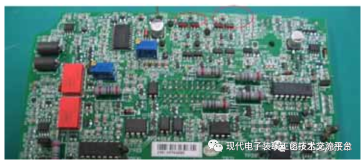
A chip capacitor located on the edge of a separation board of a certain product frequently burned out. After confirmation, it was found that the cracking of the chip capacitor was caused by the separation of the board. After powering on, the temperature caused misalignment at the fracture, leading to a fire and damage to the chip capacitor, as shown in the figure.
This account is non-profit. This article is sourced from electronic technology sharing and is for communication and learning purposes only. The text, images, and other content of this article are reprinted from the internet, and the copyright belongs to the original author. If any rights holders have objections, please contact us as soon as possible, and we will delete it promptly. The content of this article reflects the original author’s views and does not represent this public account’s endorsement of their views or responsibility for its authenticity..

WeChat group for electronic assembly process technology (Note: Company + Name)

QQ group for electronic assembly process technology (Note: Company + Name)
Press and hold to scan the QR code to follow the [Modern Electronic Assembly Process Technology] subscription account and start our shared learning journey.

Training Information:
Advanced Seminar on Reliability Design and Failure Analysis Technology for Electronic Products August 20-21, 2020 Nanjing
Advanced Seminar on SMT Welding Process Misunderstandings and Analysis Technology August 21-22, 2020 Nanjing
Advanced Seminar on Cost Control and On-Site Improvement Technology in Manufacturing August 27-28, 2020 Nanjing
Practical Case Analysis of Non-Conformance in Product Implementation Based on GJB9001C-2017 Standard August 27-28, 2020 Xi’an
Special Topic on Process Management of Weapon Equipment Development August 27-28, 2020 Luoyang
Advanced Seminar on Mechanical Structure Design and Specifications August 13-14, 2020 Nanjing
Advanced Seminar on Testability Design (DFT) Technology for Electronic Hardware Products September 17-18, 2020 Hangzhou
Advanced Seminar on Mechanical Vibration and Noise Design September 15-16, 2020 Nanjing
Advanced Seminar on DFMA – Design for Manufacturability and Assembly of Electronic Products September 17-18, 2020 Beijing
Practical Assembly Technology and Fault Analysis of Multi-Core Cable Assemblies September 24-25, 2020 Beijing
SMT Series
Causes and Solutions of SMT Defects
SMT Appearance Inspection Standards PPT – Very Good!!!
Analysis of SMT Reflow Oven Temperature Curves – Collectible Version PPT
SMT Soldering Defects and Inspection Techniques (Worth Collecting)
SMT Abnormal Handling Specifications
SMT Position Technical Training – Collectible Version
Design and Review of SMT Printed Circuit Boards (Part 1)
Design and Review of SMT Printed Circuit Boards (Part 2)
Analysis of SMT Soldering Defects (27 Phenomena)
Analysis of SMT Processes and Common Issues (Part 1)
Analysis of SMT Processes and Common Issues (Part 2)
Analysis of SMT Processes and Common Issues (Part 3)
Analysis of SMT Processes and Common Issues (Part 4)
Analysis of SMT Processes and Common Issues (Part 5)
Technical Measures for Defects in SMT (Practical Content)
Causes and Solutions of SMT Defects
Assembly and Welding Series:
Electronic Equipment Assembly Wiring Process Technology (33-page PPT)
Highest Realm of Assembly Wiring (Worth Appreciating)
Electrical Assembly Skills Technical Foundation Training
Aerospace Product Electronic Assembly Forbidden (Limited) Processes
Hand Soldering Process Technology Special Topic
Hand Soldering Process Technology Special Topic (Part 2)
Hand Soldering Process Technology Special Topic (Part 3)
Hand Soldering Techniques for Surface Mount Electronic Components
Hand Soldering Process Technology Training Materials
Common Components Hand Soldering Temperature Requirements Table
Application Guide for Electrical Connectors
Application and Selection of Low-Frequency Electrical Connectors
Electronic Wiring Process Flow Lecture
PCBA Series:
PCBA Appearance Inspection Specifications (Illustrated)
Non-Wetting and Re-Wetting in PCBA Reflow Soldering
PCBA Process and Defect Mode Analysis Technology
Modeling and Simulation Technology of PCBA Reflow Soldering Process Based on ICEPAK
PCBA Design Specifications for Manufacturability
PCBA Cold Welding Analysis
Definition, Causes, and Determination Methods of Cold Solder
Analysis and Preventive Measures for Cold Solder in Electronic Product Production
Three Prevention Series:
Selection of New Three Prevention Coating Materials for Aerospace Model Products
Three Prevention and Sealing as well as Mixed PCB Repair Technology
Three Prevention Process Technology for Assembled Printed Circuit Boards (Practical Content)
Operation Specifications and Inspection Requirements for Three Prevention Coating on Printed Circuit Boards
Three Prevention Design Process Technology – Teacher Ma Qian
Three Prevention Process Technology for Assembled Printed Circuit Boards (Practical Content)
Analysis of Common Problems and Solutions in Three Prevention Coatings
Production Management Series:
Eight Major Wastes in Lean Production – PPT
Workshop On-Site Management Topic – Worth Collecting
Lean Production (Animated Version), Very Intuitive!
Lean Production System Mind Map~ Practical Content
Production Line Balancing Analysis and Bottleneck Improvement – Essence Version
Production Planning and Material Control Technical Training Materials
8D Report Writing and Production Process Abnormal Handling Training Materials (Worth Collecting)
Lead-Free Manufacturing Technology for Lead-Free Material Production Management – Collectible Version
Standard Time Calculation and Production Line Balancing Analysis Technical Sharing
Daily Management Projects for Excellent Team Leaders (Worth Collecting)
Taguchi Method (DOE) Experimental Design Technology
On-Site Visualization Management and Kanban Design (Collectible Version)
PCB Series:
Causes and Countermeasures for PCB Solder Mask Issues
PCB Solder Mask – How to Solve Residuals on the Solder Mask Layer
PCB Reliability Design Specifications – 268 Items
Specifications for PCB Assembly and Soldering Process Technology
Common Appearance Defects and Cause Analysis of PCBs (Part 1)
Common Appearance Defects and Cause Analysis of PCBs (Part 2)
Basic Knowledge of PCBs (Part 1)
Basic Knowledge of PCBs (Part 2)
Basic Knowledge of PCBs (Part 3)
PCB Design Delivery Checklist – Collectible Version
PCB Appearance Inspection Standards – Hundreds of Items
Analysis of PCB Explosions (Practical Content)
Quality Series:
How to Be a Good Quality Inspector – Please Keep This PPT Safe!
IPQC (Process Control) Inspection Skills – Practical Content
Analysis of Electronic Component Failure Technologies – Essence
Group Communication:
WeChat Group for Electronic Assembly Process Technology
Book Recommendations:
Surface Mount Technology (SMT) Basic Process Book Recommendations