Simply put, what is PCB? PCB = printed circuit board; the Chinese name is 印制电路板, also known as printed circuit board, is an important electronic component, serving as the support for electronic components and the carrier for electrical connections between electronic components. Because it is made using electronic printing techniques, it is called a ‘printed’ circuit board.
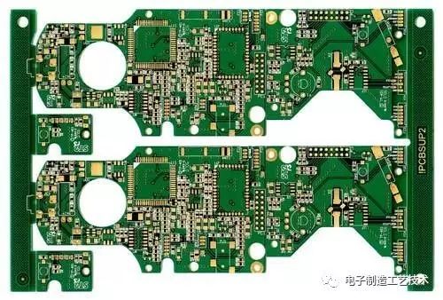
What is PCBA? PCBA = assembly of PCB. Various electronic components are assembled onto the circuit board through surface mount technology. Next is box assembly, which involves assembling the completed PCB with the enclosure and other components to form the finished product. In other words, a bare PCB goes through the SMT process, and then through the DIP plug-in process, collectively referred to as PCBA. This is a common term used in China, while in Europe and America, it is written as PCB’A, with a slant point added. PCBA is the PCB that has components mounted on it.
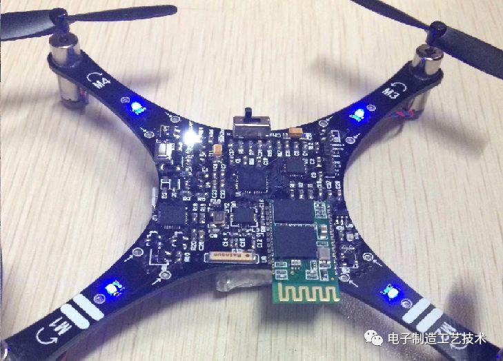
What is the difference between PCB and PCBA? PCB refers to the circuit board, while PCBA refers to the assembly of components on the circuit board, specifically the SMT process. One is a finished board while the other is a bare board. PCB (Printed Circuit Board) is made from epoxy glass resin material and is classified into 4, 6, or 8 layers based on the number of signal layers, with 4 and 6 layers being the most common. Chip components are mounted on the PCB. PCBA can be understood as a finished circuit board, meaning all processes on the circuit board must be completed for it to be considered PCBA. PCBA = Printed Circuit Board + Assembly. In other words, a bare PCB goes through the SMT process and then the DIP plug-in process, collectively referred to as PCBA. PCB (Printed Circuit Board) is the abbreviation for printed circuit boards, usually made on insulating material, designed to create conductive patterns for printed circuits or a combination of both. The conductive patterns providing electrical connections between components on the insulating substrate are referred to as printed circuits. Thus, the finished board of printed circuits or printed lines is called a printed circuit board, also known as a printed board or printed circuit board.
PCBA process is a combination of SMT processing and DIP processing, which can be divided into single-sided SMT assembly process, single-sided DIP insertion process, single-sided mixed assembly process, single-sided assembly and insertion mixed process, double-sided SMT assembly process, and double-sided mixed assembly process, etc.
PCBA process involves various stages including carrier board, printing, chip mounting, reflow soldering, insertion, wave soldering, testing, and quality inspection, as detailed in the following PCBA process flowchart.
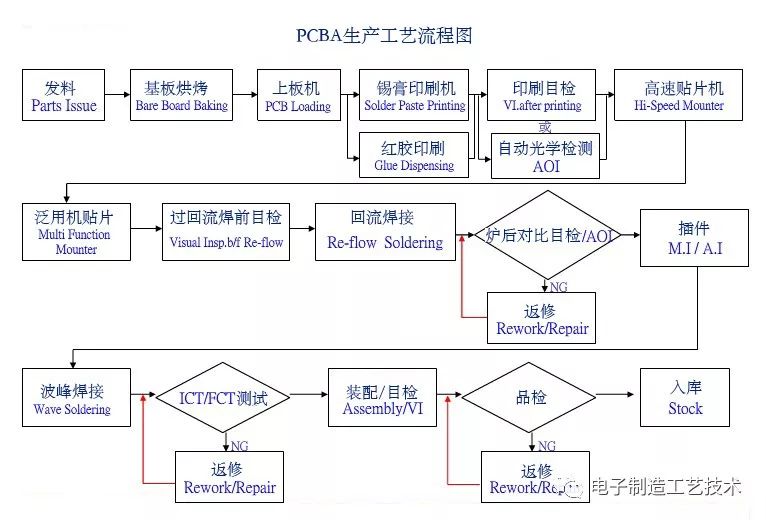
PCBA process flowchart
Different types of PCB boards have varying process flows; below are detailed descriptions of their differences.
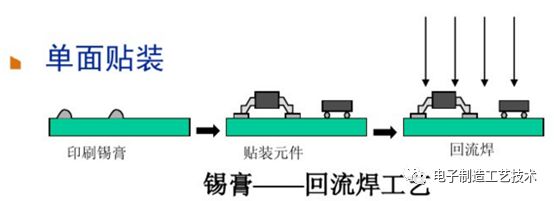
1. Single-sided SMT assembly
Solder paste is added to the component pads, and after the solder paste is printed on the bare PCB, it is mounted with related electronic components through reflow soldering.
2. Single-sided DIP insertion
The PCB board requiring insertion is manually inserted with electronic components by production line workers and then passed through wave soldering for fixing. However, wave soldering has a lower production efficiency.
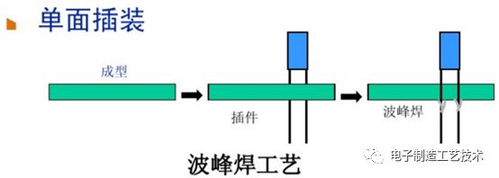
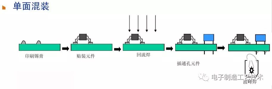
3. Single-sided mixed assembly
The PCB board undergoes solder paste printing, mounts electronic components, and then is fixed through reflow soldering. After quality inspection, it undergoes DIP insertion and then wave soldering or manual soldering. If through-hole components are few, manual soldering is recommended.
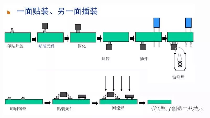
4. Mixed assembly of surface mount and insertion
Some PCB boards are double-sided, with one side for surface mount and the other for insertion. The assembly process for surface mount and insertion is the same as single-sided processing, but the PCB board requires fixtures when passing through reflow soldering and wave soldering.
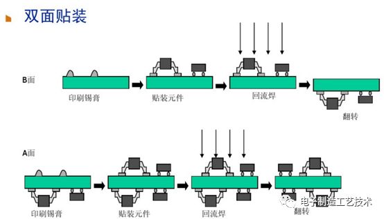
5. Double-sided SMT assembly
Some PCB board design engineers use double-sided assembly to ensure the aesthetics and functionality of the PCB board. IC components are arranged on side A, while surface mount components are placed on side B. This fully utilizes PCB board space, minimizing PCB area.
6. Double-sided mixed assembly
Double-sided mixed assembly can be done in two ways: the first involves PCBA assembly with three heating processes, which is less efficient, and using red glue for wave soldering has a low qualification rate, thus not recommended. The second method is suitable for cases with many double-sided SMD components and few THT components, where manual soldering is recommended. If THT components are numerous, wave soldering is suggested.
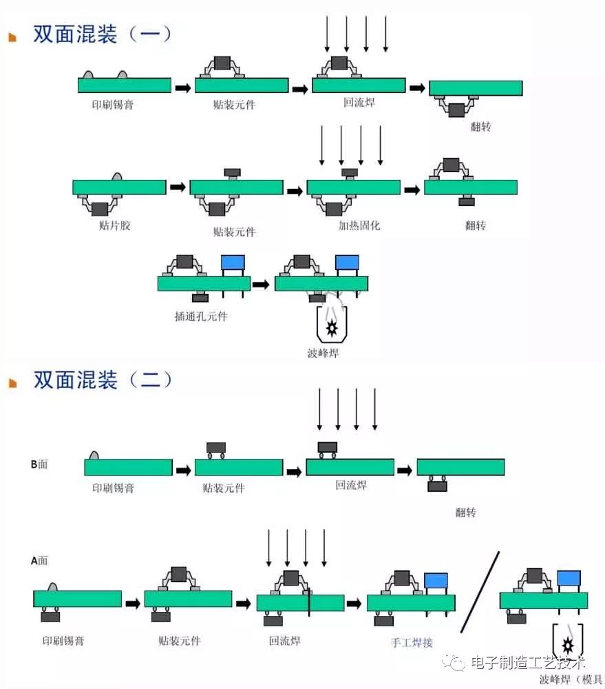
The above is a simplified overview of the PCBA assembly process for printed circuit boards, presented through images and text. As the PCBA assembly process and production methods are gradually optimized, the defect rate continues to decrease, ensuring the production of high-quality finished products. The quality of all solder joints for the electronic components mentioned above determines the quality of the PCBA board. Therefore, when electronic manufacturers seek PCBA assembly suppliers, it is best to require experienced and high-level processing equipment.
Extract the essence, discard the dross, strengthen the foundation, and promote innovation
Note: Many fans have not yet developed the habit of liking and sharing after reading; I hope everyone will like and share while reading to show encouragement! It’s really not easy for a team to persist for a long time; we have thought of giving up many times. Persistence is a belief, and focus is an attitude!


Disclaimer: This article is an original work edited from materials collected online, with copyright belonging to the original author. If reprinted, please indicate the source and mark the reprint origin. If any works are involved, please contact us.
If you need soft articles or image advertising business cooperation, please contact us.