PCBA Process Flow
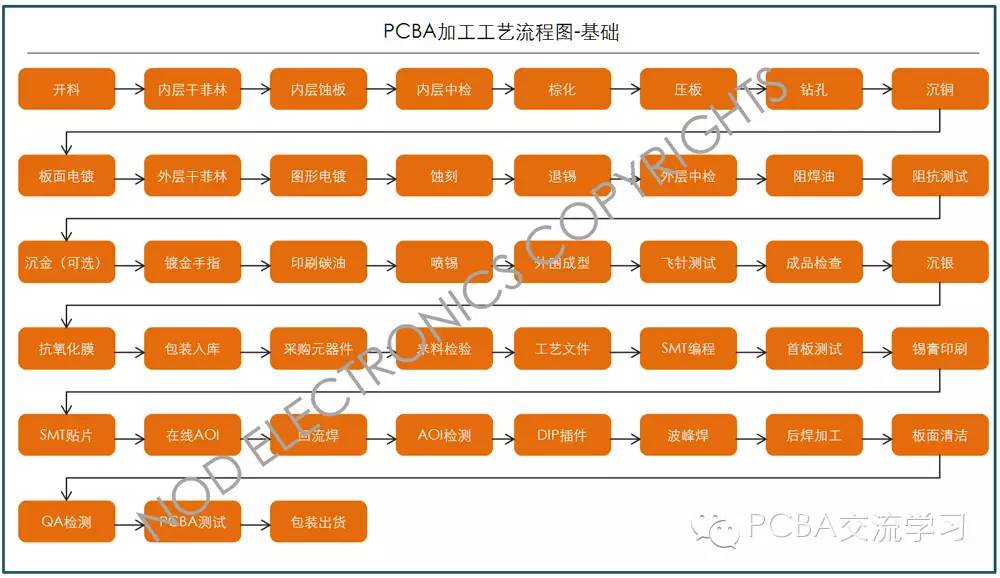
The PCBA process is quite complex and typically goes through nearly 50 procedures, including circuit board manufacturing, component procurement and inspection, SMT assembly, DIP insertion, PCBA testing, programming, and packaging. Among these, the circuit board manufacturing consists of 20 to 30 procedures, making it extremely complex. The following diagram illustrates the PCBA processing workflow in detail, allowing you to quickly acquire relevant professional knowledge.
PCBA Process Flow Diagram
Circuit Board Manufacturing Processes and Equipment
Circuit board equipment includes plating lines, copper sinking lines, DES lines, SES lines, cleaning machines, OSP lines, nickel-gold sinking lines, presses, exposure machines, ovens, AOI, board warping flatness machines, edge grinding machines, material cutting machines, vacuum packaging machines, milling machines, drilling machines, air compressors, tin spraying machines, CMI series, photoplotters, etc.
Circuit boards can be classified into single-sided, double-sided, and multi-layer printed boards based on the number of conductor layers. The basic manufacturing process for single-sided boards is as follows:
Foil board –> Material cutting –> Board baking (to prevent deformation) –> Molding –> Cleaning and drying –> Film application (or screen printing) –> Exposure and development (or anti-corrosion ink) –> Etching –> Film removal –> Electrical continuity testing –> Cleaning treatment –> Screen printing solder mask (green ink) –> Curing –> Screen printing markings –> Curing –> Drilling –> Shaping processing –> Cleaning and drying –> Inspection –> Packaging –> Finished product.
The basic manufacturing process for double-sided boards is as follows:
Pattern Plating Process
Foil board –> Material cutting –> Punching reference holes –> CNC drilling –> Inspection –> Deburring –> Chemical copper plating –> Electroplating copper –> Inspection –> Board brushing –> Film application (or screen printing) –> Exposure and development (or curing) –> Inspection and repair –> Pattern plating (Cn + Sn/Pb) –> Film removal –> Etching –> Inspection and repair –> Plug nickel-gold plating –> Hot melt cleaning –> Electrical continuity testing –> Cleaning treatment –> Screen printing solder mask –> Curing –> Screen printing markings –> Curing –> Shaping processing –> Cleaning and drying –> Inspection –> Packaging –> Finished product.
SMOBC Process has the main advantage of resolving the phenomenon of solder bridging short circuits between fine lines, and due to the constant lead-tin ratio, it offers better solderability and storage than hot melt boards. The SMOBC process, which uses pattern plating to remove lead-tin, is similar to the pattern plating process, with changes occurring only after etching. Double-sided copper foil boards –> Follow the pattern plating process to the etching step –> Remove lead-tin –> Inspection –> Cleaning –> Solder mask pattern –> Plug nickel-gold plating –> Tape application on plugs –> Hot air flattening –> Cleaning –> Screen printing markings –> Shaping processing –> Cleaning and drying –> Finished product inspection –> Packaging –> Finished product.
SMT Assembly Process
1. Create SMT production process documents based on customer Gerber files and BOM lists, generating SMT coordinate files.
2. Inventory all production materials to ensure completeness, prepare a completeness list, and confirm the production PMC plan.
3. Perform SMT programming and create the first board for verification to ensure accuracy.
4. Produce laser stencils according to SMT processes.
5. Conduct solder paste printing, ensuring that the printed solder paste is uniform, of good thickness, and consistent.
6. Use SMT placement machines to mount components onto the circuit board, performing online AOI automatic optical inspection as necessary.
7. Set the perfect reflow soldering oven temperature curve, allowing the circuit board to pass through the reflow soldering, converting solder paste from paste to liquid and then to solid, achieving good soldering after cooling.
8. Conduct necessary IPQC inspections.
9. The DIP insertion process involves inserting through-hole components into the circuit board, which then passes through wave soldering for soldering.
10. Necessary post-oven processes, such as trimming leads, post-soldering, board surface cleaning, etc.
11. QA conducts comprehensive testing to ensure quality is acceptable.
PCBA Testing
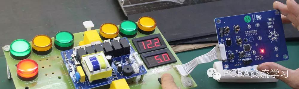
PCBA testing is the most critical quality control stage in the entire PCBA processing procedure. It requires strict adherence to PCBA testing standards and testing points on the circuit board according to the customer’s test plan (Test Plan). PCBA testing includes five main forms: ICT testing, FCT testing, burn-in testing, fatigue testing, and testing under severe conditions. Among these, ICT (In-Circuit Test) testing mainly includes checking circuit continuity, voltage and current values, fluctuation curves, amplitude, noise, etc.; while FCT (Functional Circuit Test) testing requires programming the IC, simulating the functionality of the entire PCBA board to identify issues in hardware and software, and providing necessary production fixtures and test racks; burn-in testing primarily involves powering the PCBA board and electronic products for an extended period, observing any failures before mass production; fatigue testing mainly involves sampling the PCBA board and conducting high-frequency, long-duration operations to observe failures, such as clicking a mouse 100,000 times or switching an LED on and off 10,000 times, to test the probability of failure and provide feedback on the operational performance of the PCBA board; testing under severe conditions mainly involves exposing the PCBA board to extreme temperatures, humidity, drops, splashes, and vibrations to obtain random sample test results, thereby inferring the reliability of the entire batch of PCBA products.